IN Brief:
- A ten-month Cardiff programme will develop a fabrication process for thin-film lithium niobate photonic integrated circuits.
- Finchetto attributes potential 700-fold latency and 20-fold power improvements to its optical switching approach; independent supporting benchmarks were not disclosed.
- The project uses university cleanroom facilities, but neither a qualified volume process nor a commercially manufactured switch has been announced.
Finchetto has started a ten-month programme in Cardiff to develop a repeatable manufacturing process for photonic integrated circuits based on thin-film lithium niobate. The work will use Cardiff University’s Institute for Compound Semiconductors cleanroom facilities and is directed at the optical packet-switching hardware being developed by the UK company. No qualified volume production line or commercially fabricated switching chip has yet been announced under the programme.
The project is supported by a grant through the Investor Partnerships Programme and private investment from the Development Bank of Wales. Finchetto has operations in Cardiff as well as an office and laboratory in Guildford, Surrey. The use of shared cleanroom infrastructure allows the process design to be tested without assuming that Finchetto already operates a dedicated semiconductor factory.
Photonic integrated circuits guide and manipulate light through patterned structures on a chip, allowing functions that would otherwise depend on discrete optical components to be combined on a smaller substrate. Thin-film lithium niobate is attractive because an applied electrical field can change its optical properties. The electro-optic effect provides a route to controlling or switching light without having to perform every data-routing operation in an electronic processing circuit.
Finchetto is developing optical packet switching for data networks, including AI computing infrastructure, and says its proposed architecture could substantially reduce signal conversions. In a conventional electronic switching path, an optical signal may be converted into an electrical representation for processing and then converted back into light for onward transmission. Finchetto reports a potential 700-fold latency reduction and 20-fold power reduction against traditional electro-optical network switches. Those are supplier-reported comparisons: the 14 October company-attributed announcement provides neither benchmark methodology nor independently verified measurements, and the figures are not results from the proposed Cardiff manufacturing process. Reducing conversions may save energy and time, but the actual result depends on switch architecture, buffering, electrical controls and the traffic being carried.
Repeatable fabrication of optical waveguides and switching structures requires control of feature dimensions, material quality, optical coupling loss and the relationship between electrical drive structures and optical paths. Those process parameters must be established before the proposed architecture can be manufactured consistently. Variations introduced by patterning, etching or subsequent processing can change insertion loss and device response. Those characteristics must be measured across wafers and repeat builds before a reliable production process can be established.
Thin-film lithium niobate structures require fabrication and optical-characterisation steps that differ from a conventional silicon logic manufacturing process. The optical circuit must preserve the intended waveguide geometry and material characteristics while accommodating any electrodes, optical interfaces and packaging required by the switch. Matching laboratory performance to a manufacturable sequence can involve changes to layout, tolerances and test structures. Finchetto has not publicly specified production yield, wafer volume or qualified process capability for this new programme.
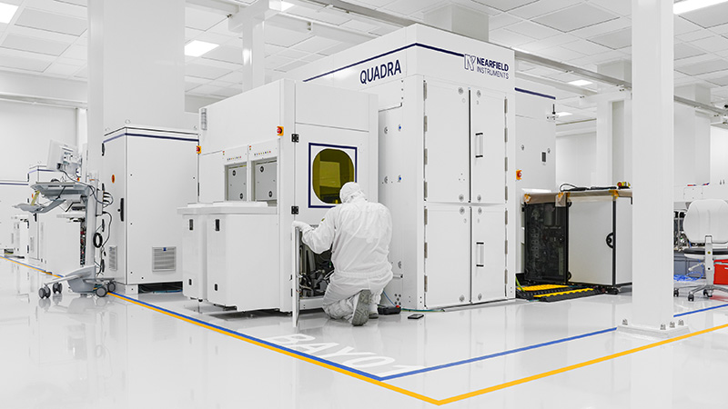
Cardiff University’s Institute for Compound Semiconductors offers open-access research and process-development infrastructure, including pilot-scale fabrication capability. That provides a setting in which an industrial design can be evaluated against available cleanroom processes and adjusted as results emerge. The facility’s existing capabilities are not evidence that Finchetto has commissioned a dedicated volume production line or secured manufacturing orders for the switch.
The photonic die must also be connected to optical fibres, control electronics and stable packaging before it can form part of a deployable switching system. High-speed optical systems need interfaces to fibres or other optical components, packaging that maintains alignment, electrical connections for control and, where applicable, thermal stability. Insertion loss through couplers and switches affects how much optical power must be supplied elsewhere in the link. Reliability and production test methods become important when individual devices are combined into larger networks carrying time-sensitive traffic.
Finchetto has previously discussed pilot deployment of its optical networking technology, but a pilot programme and a reproducible chip-manufacturing process are separate steps. Testing network behaviour can demonstrate an architectural function without proving that the underlying components can be fabricated and assembled at commercial yield. Conversely, a stable device process must still be qualified within the intended switching system before network-level performance claims can be generalised.
The ten-month programme establishes a period for developing and evaluating the Cardiff fabrication route, but no qualified process yield, product test result or volume shipment date has been announced. The first meaningful technical milestones will be device characterisation and repeatability across fabrication runs; system qualification and commercial production remain separate steps.