
IN Brief:
- CCRAFT has raised $7.8m to scale thin-film lithium niobate photonic chip manufacturing.
- The CSEM spin-off operates an independent TFLN photonic chip foundry in Neuchâtel.
- The company plans to expand production capacity to as much as 2,000 wafers per month by 2030.
CCRAFT has raised $7.8m to scale industrial manufacturing of thin-film lithium niobate photonic chips in Neuchâtel, Switzerland.
The CSEM spin-off closed an oversubscribed CHF 6.3m funding round led by QBIT Capital, with participation from Zürcher Kantonalbank, Apprecia Capital, Spacewalk, Blue Wonder Ventures, and a European AI infrastructure operator. Combined with more than $3.5m already secured in public and cantonal support, the company now has around $11.3m in fresh capital to expand its manufacturing platform.
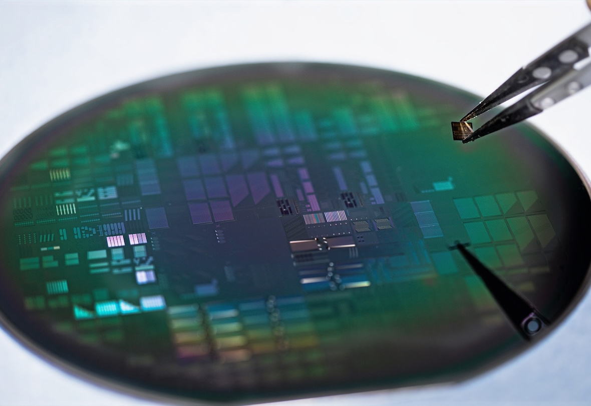
CCRAFT operates an independent foundry for thin-film lithium niobate, or TFLN, photonic chips. The technology was developed over more than six years at CSEM before being commercialised by CCRAFT, which has been operating from Neuchâtel since April 2025. The company already produces devices for customers across four continents and plans to scale capacity to as much as 2,000 wafers per month by 2030.
TFLN can support high-speed, energy-efficient optical modulation, making it relevant to AI data centres, communications infrastructure, quantum systems, aerospace, sensing, and advanced photonic integrated circuits. As AI infrastructure grows, the ability to move data quickly and efficiently between processors, memory, boards, racks, and clusters is becoming as important as raw compute throughput.
The same cluster of constraints appeared in the latest quarterly electronics market analysis, where memory, packaging, optics, edge AI, power delivery, and design automation all formed part of the same technology bottleneck. CCRAFT’s funding sits directly inside that pattern. Photonics is being pulled into data-centre architecture, high-speed interconnect, and system-level efficiency planning.
Electrical interconnect remains dominant across most systems, but its limits are increasingly visible in high-bandwidth environments. As data movement rises, power per bit, latency, signal integrity, reach, and thermal loading all become harder to manage with conventional approaches alone. Optical links can reduce some of those constraints, although they introduce their own challenges around integration, packaging, alignment, test, yield, and manufacturing scale.
A foundry model gives the technology a clearer industrial route. Photonic chip designs cannot move into broad adoption if manufacturing remains confined to pilot lines and bespoke research flows. Customers need predictable process capability, design rules, repeatable wafer-level production, packaging routes, and qualification evidence. Scaling TFLN production in Switzerland gives the European photonics ecosystem a more practical route from device concept to deployable hardware.
The wider market opportunity is substantial. The global photonic integrated circuit market is estimated at $15bn to $20bn, with the addressable market for TFLN-based chips expected to reach several billion dollars by 2030. Those figures will depend on industrialisation rather than laboratory performance alone. A photonic device has to be produced, packaged, tested, and supplied at a level that system builders can trust.
Europe has strong research positions in photonics, compound semiconductors, sensing, and high-reliability systems, while scale-up remains the recurring difficulty. CCRAFT’s funding addresses that gap at the manufacturing layer and gives Switzerland a more visible role in the race to industrialise optical technologies for AI and high-performance data movement.
Reaching 2,000 wafers per month will require equipment, process control, yield learning, skilled staff, packaging relationships, customer qualification, and stable materials supply. If the company can convert capital into repeatable output, photonic system developers will have a stronger European route to TFLN chips at a point when optics is entering the mainstream electronics roadmap.

