IN Brief:
- Coherent is sampling 300mm high-thermal-conductivity SiC substrates to AI semiconductor partners.
- The company says the material can improve heat spreading by up to 25% while remaining compatible with established semiconductor manufacturing platforms.
- Customer evaluation will test thermal performance, integration behaviour, and manufacturability before any progression towards volume production.
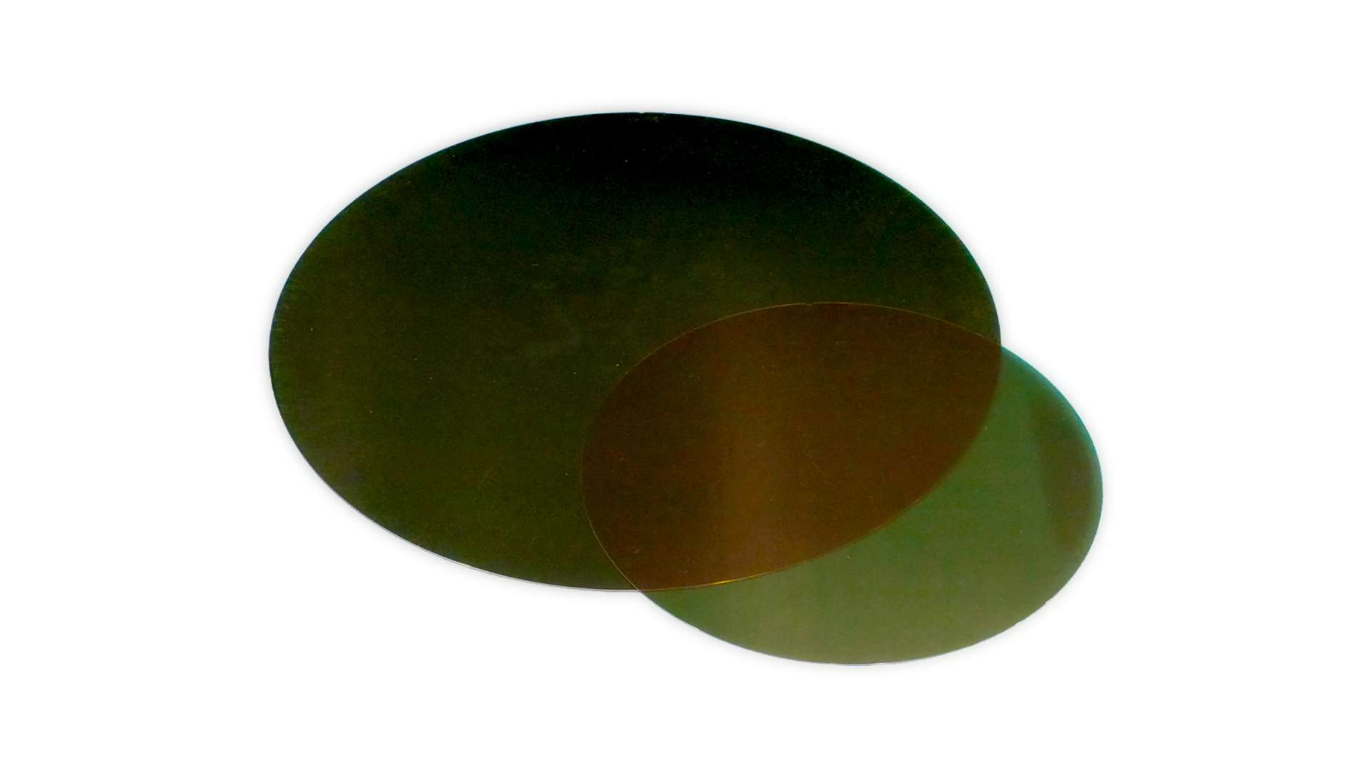
Coherent has begun customer sampling of 300mm high-thermal-conductivity silicon carbide substrates to AI semiconductor partners, taking the material platform beyond internal development and into external package evaluation. The substrates are intended for heat spreaders and related thermal-management structures in AI and high-performance computing hardware, where rising processor power density is increasing the thermal load carried by package materials.
Coherent says the substrates can improve heat spreading by up to 25% compared with current solutions while remaining compatible with established semiconductor manufacturing platforms. The company is producing the material through a vertically integrated process covering SiC crystal growth, wafering, polishing, and characterisation, giving it control over several properties that will have to remain consistent if the platform progresses towards volume production.
The 300mm format is significant because advanced semiconductor packaging is increasingly being developed around wafer-scale processes and equipment designed for larger substrates. A material may offer strong thermal conductivity in isolation, but package manufacturers still have to manage flatness, surface quality, mechanical strength, thermal expansion, bonding, handling, and yield across a full wafer before it becomes useful in a production flow.
AI accelerators have intensified that problem by concentrating more compute and memory bandwidth into packages with limited room for conventional thermal solutions. Heat generated at the die has to cross several material interfaces before it reaches a cold plate, liquid loop, or air-cooled heat sink, and localised hotspots can limit frequency, reliability, or packaging density before the external cooling system reaches its own capacity.
A high-conductivity SiC heat spreader addresses that part of the thermal path close to the semiconductor. It does not replace system-level cooling, but it can distribute heat over a larger area before that energy reaches the next interface, reducing temperature gradients around high-power regions and giving package designers more control over where heat enters the cooling structure.
Coherent is positioning the material around a combination of thermal conductivity, mechanical strength, and thermal stability. Those properties have to survive repeated heating and cooling while maintaining tight dimensional tolerances, particularly in advanced packages where processors, memory stacks, interposers, and interconnect structures are assembled within increasingly compact geometries.
Customer sampling now shifts the evaluation burden towards semiconductor and packaging companies. They can measure wafer quality, bonding behaviour, thermal resistance, assembly yield, mechanical compatibility, and reliability against their own package designs rather than relying on supplier-level material data. The resulting work is likely to determine whether the claimed heat-spreading improvement survives the additional interfaces and constraints of a complete package.
The move also tests the manufacturing case for 300mm SiC outside its established use in power electronics. Producing large, consistent SiC substrates is technically demanding, and a thermal-management application will have to justify its cost against competing heat-spreader materials, packaging changes, and improvements elsewhere in the cooling stack. The engineering advantage therefore has to be measured at package and system level rather than from bulk material conductivity alone.
Coherent’s existing control of crystal growth and wafer processing gives it a route to adjust the material as customers report integration results. Surface preparation, thickness, defect levels, and mechanical characteristics can all influence downstream assembly, while a repeatable 300mm process will be necessary if the technology is to move from evaluation quantities into the volumes expected for mainstream AI infrastructure.
The sampling milestone places those questions with customers at a useful point in the technology cycle. AI hardware developers are already adopting more aggressive liquid cooling and denser package architectures, so any new heat-spreader material will be assessed against systems that are changing quickly rather than a fixed reference design.
Coherent now has to demonstrate that its SiC substrates improve thermal performance without introducing a new manufacturing penalty elsewhere in the package. If customer trials confirm that balance, the 300mm platform would give package designers another material option for moving heat away from the increasingly concentrated power densities of next-generation processors.