IN Brief:
- Avicena has begun shipping 1Tbps LightBundle evaluation kits to AI infrastructure developers.
- The system combines 335 microLED channels running at up to 3Gbps each with a 335-element photodiode array.
- External evaluation will test signal integrity, power, crosstalk, packaging, and link behaviour against competing AI interconnect technologies.
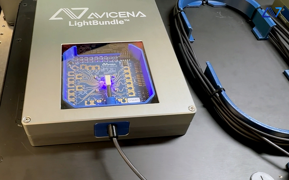
Avicena has begun shipping 1Tbps LightBundle microLED optical-interconnect evaluation kits to customers and partners developing AI infrastructure. The shipment follows the platform’s introduction and demonstration at OFC in March 2026 and brings the technology to terabit-class operation in customer laboratories rather than leaving it at supplier demonstrations.
The latest kit uses a 335-channel microLED array, with each data channel operating at up to 3Gbps, coupled through Avicena’s multicore fibre to a 335-element integrated photodiode array. Together, those parallel channels provide up to 1Tbps of aggregate raw throughput while avoiding the laser transmitters used in conventional optical links.
Avicena is targeting short-reach connections inside AI systems, including accelerator-to-accelerator, accelerator-to-memory, processor, and switch links. Those connections are becoming harder to scale electrically as bandwidth rises because copper traces and cables face increasing loss, equalisation, routing-density, and power constraints over the distances found within large compute systems.
Optical links can extend reach and reduce some electrical losses, but they introduce another set of packaging and power trade-offs. Avicena’s approach uses dense microLED transmitter arrays rather than conventional laser sources, combining many comparatively low-rate optical channels instead of pushing a small number of lanes to extremely high serial data rates.
That parallel architecture shifts the design problem towards array integration, channel uniformity, fibre alignment, receiver matching, and dense packaging. A 1Tbps headline rate is therefore only one part of the evaluation. Engineers need to establish whether hundreds of channels can operate predictably together while meeting the power, crosstalk, thermal, and manufacturing requirements of a practical interconnect.
The evaluation kit includes host-interface boards, diagnostics, and a graphical interface for measuring optical signal integrity, link budget, eye quality, crosstalk, power efficiency, and bit-error-rate performance. Those measurements allow customers to compare the technology with electrical and optical alternatives under their own operating conditions rather than relying on demonstration data generated by the supplier.
The kit is intended as an engineering platform rather than a finished interconnect module. Its purpose is to expose the electrical and optical behaviour of the LightBundle transceivers while giving customers access to repeatable diagnostics, so package and system teams can investigate the technology before committing to a specific mechanical or board architecture. That separation is useful at this stage because potential applications range from board-level links to much tighter integration around accelerators and memory.
The August shipment is distinct from Avicena’s March introduction of the LightBundle eKit. The earlier platform demonstrated 512Gbps operation and established the evaluation architecture; the new kit brings the aggregate rate to 1Tbps and places that configuration into external laboratories. That makes the current development a customer-evaluation milestone rather than a second launch of the same hardware concept.
Moving optical connectivity closer to processors and memory also changes the reliability requirements placed on the interconnect. Links embedded deep inside a compute system may be harder to service than conventional pluggable network optics and have to operate alongside high-power silicon, rapidly changing thermal loads, and dense mechanical assemblies.
MicroLED transmitters are intended to offer a different reliability and power profile from laser-based architectures, but customer evaluation will determine whether those advantages persist once the technology is integrated with real package, board, and system constraints. Connector geometry, fibre routing, device ageing, temperature variation, and manufacturing tolerance will all affect whether laboratory performance can translate into repeatable production hardware.
AI system designers are considering several paths to greater interconnect bandwidth, including improved electrical I/O, co-packaged optics, silicon photonics, and optical technologies positioned progressively closer to compute silicon. No single approach has yet removed the trade-off between reach, energy per bit, density, cost, and serviceability.
Avicena’s 1Tbps shipments put microLED connectivity into that comparison with hardware that customers can measure directly. The next evidence will come from those system-level evaluations, where the technology has to prove that a highly parallel optical link can deliver its bandwidth advantage without simply relocating complexity into fibre alignment, packaging, or manufacturing.