IN Brief:
- Internal polarisation fields in conventional c-plane GaN quantum wells separate electrons and holes, reducing efficiency and wavelength stability.
- InGaN/AlGaN digital-alloy barriers cut the measured field to 0.5MV/cm and delivered peak external quantum efficiency of 15%.
- The growth process was transferred to a four-inch industrial MOCVD platform while also reducing micro-LED sidewall sensitivity.
Researchers led by Jilin University have demonstrated InGaN/AlGaN digital-alloy quantum barriers that reduce the internal polarisation field in c-plane III-nitride LEDs while retaining an epitaxial route compatible with industrial MOCVD equipment. The resulting blue devices reached peak external quantum efficiency of 15% and showed substantially stronger lateral carrier confinement than conventional InGaN/GaN quantum-well structures.
The work tackles a long-standing limitation of polar c-plane GaN. Spontaneous and piezoelectric polarisation generates an electric field across the quantum wells, tilting the band structure and separating electron and hole wavefunctions. The resulting quantum-confined Stark effect reduces radiative recombination and can shift the emission wavelength as carrier density changes.
Non-polar and semi-polar GaN orientations can reduce that field, but their substrates and epitaxy are generally more difficult and expensive to manufacture. The research team instead retained the conventional polar plane and changed the quantum-barrier structure surrounding the InGaN wells.
The digital alloy consists of alternating InGaN and AlGaN layers roughly one nanometre thick. Rather than growing one quaternary InAlGaN layer, the structure creates an effective material whose average composition and polarisation can be tuned through the individual layer thicknesses and growth sequence.
Growth chemistry proved critical. The researchers tested several pulse modes for ammonia delivery during MOCVD and found that a modulated-flow approach improved interface quality while reducing nitrogen-related defects and unwanted indium incorporation in the AlGaN layer.
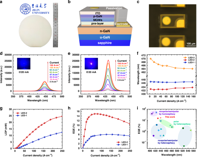
Measurements on the optimised multiple-quantum-well structure produced a calculated polarisation electric field of 0.5MV/cm, compared with 2.0MV/cm for the conventional InGaN/GaN reference. Time-resolved photoluminescence also showed much shorter carrier lifetimes, consistent with greater overlap between electron and hole wavefunctions.
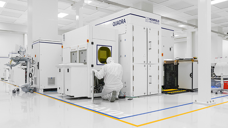
The process was then transferred onto a Veeco K465I industrial MOCVD platform for four-inch wafer growth. That step is important because epitaxial improvements developed on small research reactors can become considerably harder to reproduce once gas distribution, thermal uniformity, loading, and wafer-scale process control enter the equation.
Devices produced using the optimised structure reached 15% peak EQE. Efficiency remained above 10% at 250A/cm², where optical output reached 25mW, while the emission wavelength shifted by only 0.3nm across the reported current-density range compared with 5.9nm for the conventional reference device.
The 15% figure is below the best larger conventional blue LEDs, but that is not the comparison being made. The authors report it as the highest EQE among the heteroepitaxial weak-polarisation-field devices considered in their study, while retaining the manufacturing advantages of a polar c-plane substrate.
Lateral carrier behaviour gives the architecture another potential advantage for micro-LEDs. As pixel dimensions shrink, carriers can diffuse towards etched sidewalls where defects create non-radiative recombination paths. Shorter lateral diffusion reduces the proportion of carriers reaching that damaged perimeter.
The researchers fabricated devices between 10µm × 10µm and 60µm × 60µm to examine that scaling effect. Their analysis indicates that the weak-field structure reduced sidewall sensitivity by approximately 50% compared with a conventional InGaN/GaN LED, supporting the case for combining polarisation engineering with established micro-LED sidewall treatments.
Manufacturing still involves a wider set of constraints. Epitaxial uniformity, lithography, etch damage, passivation, contacts, colour integration, transfer or monolithic backplane integration, and final display yield can all overwhelm a gain made inside the quantum wells if they are not controlled to comparable tolerances.
The useful result is therefore the combination rather than any one record number: lower internal field, improved wavelength stability, stronger carrier confinement, and transfer onto a four-inch production-type MOCVD reactor. If the process remains uniform as wafer diameter and manufacturing volume rise, digital-alloy barriers offer a route to improving micro-LED scaling without abandoning the c-plane GaN infrastructure already used by the industry.