IN Brief:
- Taiyo Holdings and imec formed three RDL layers with 700nm critical dimensions for both interconnects and vias on 300mm wafers.
- FPIM is a negative-tone i-line photosensitive insulating material developed for fine-pitch dual-damascene redistribution processing.
- Development now targets 500nm or smaller dimensions alongside continuing electrical-reliability and long-term performance work.
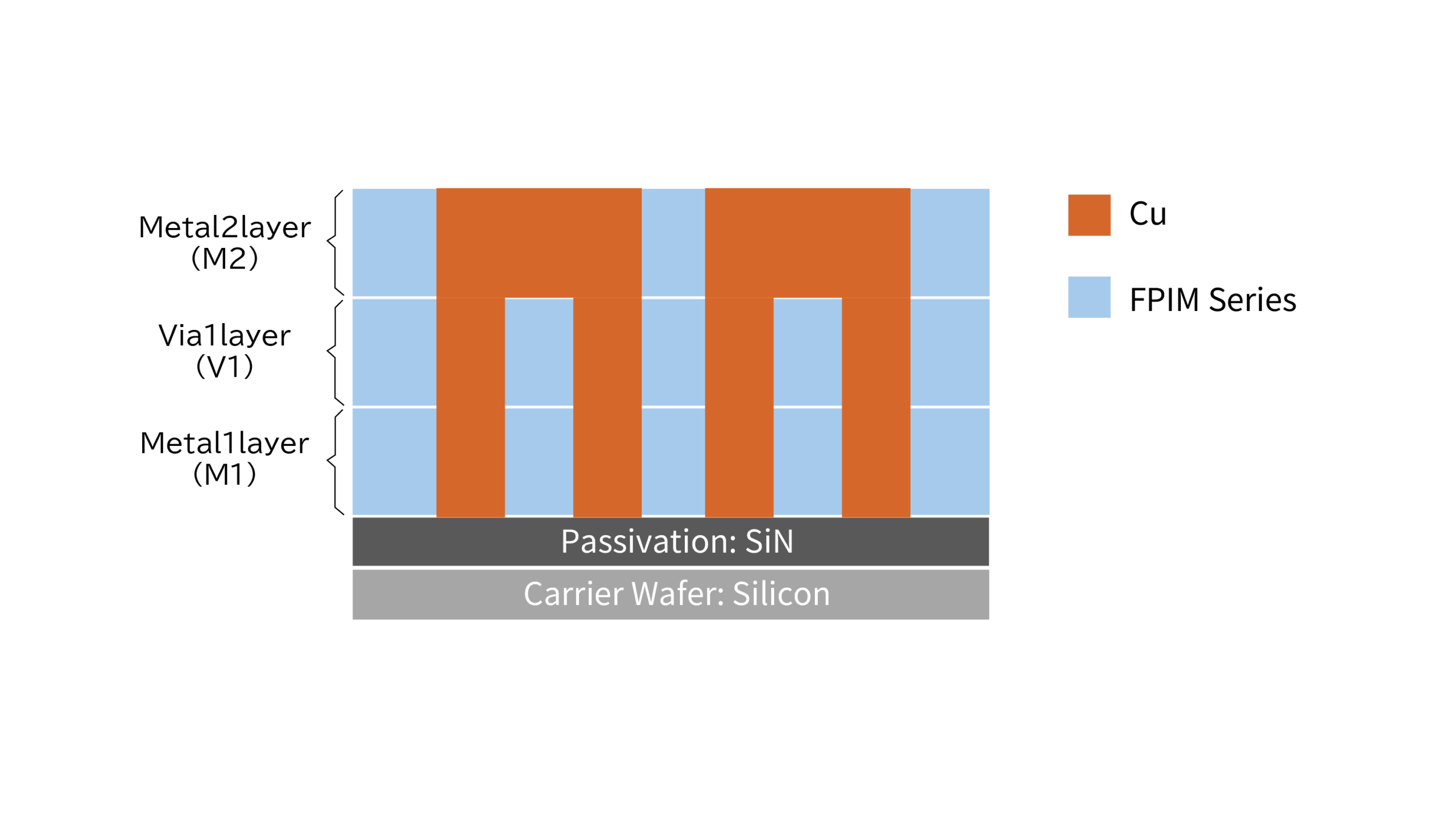
Taiyo Holdings and imec have formed a three-layer redistribution structure with 700nm critical dimensions for both interconnects and vias on 300mm wafers using Taiyo’s FPIM photosensitive dielectric.
The work was presented at IEEE ESTC 2026 in Helsinki and advances a joint programme that reached 1.6µm wiring dimensions in 2025. Electrical evaluation of the latest 700nm metal-one layer showed favourable leakage-current and resistance characteristics, while the material was also found to be compatible with chemical mechanical planarisation.
FPIM is a negative-tone i-line photosensitive insulating material intended for fine-pitch redistribution layers using a dual-damascene process. Taiyo and imec began joint development in October 2022 as package interconnect dimensions moved closer to the regime traditionally associated with wafer fabrication.
Redistribution layers reroute electrical connections across a chip or package, allowing die pads to connect to a different pitch and geometry at the package interface. Their density becomes increasingly important as systems combine chiplets, high-bandwidth memory, accelerators, RF devices, and silicon produced on different process nodes.
Conventional RDL manufacture commonly uses a semi-additive process in which a thin seed layer is deposited before selected areas are electroplated to build the required metal pattern. As line widths and spacing contract, maintaining plating profile and dimensional control becomes progressively more difficult.
Dual damascene reverses part of that sequence. Trenches and vias are patterned into the dielectric before metal fills the resulting structures, followed by planarisation of the wafer surface. The process is established in semiconductor interconnect manufacture, but applying similar principles to advanced packaging requires dielectric materials capable of resolving small structures across comparatively large areas.
In 2025, Taiyo and imec demonstrated a three-layer structure with 1.6µm wiring dimensions on 300mm wafers. The latest work takes both wiring and via dimensions to 700nm, more than halving the earlier wiring figure and moving the process into the submicron range.
That reduction is useful because package wiring increasingly has to carry signal densities that would previously have remained within a monolithic die. If the redistribution layer cannot scale alongside the number of die-to-die connections, packaging becomes an electrical and physical bottleneck even when the silicon itself can support higher interface density.
The development sits alongside wider work on heterogeneous integration. Imec’s 300mm RF silicon interposer programme, for example, combines fine interconnect, embedded passives, and chiplet assembly as package structures take a more active role in system performance.
FPIM has not yet completed the qualification work needed to treat 700nm redistribution as a volume-production process. Taiyo says it will continue evaluating long-term electrical characteristics and reliability while targeting critical dimensions of 500nm or below.
Those tests will have to address more than nominal resolution. Adhesion, dielectric stability, moisture behaviour, thermal cycling, planarisation tolerance, defect density, and compatibility with subsequent metallisation all influence whether a fine feature demonstrated on an evaluation wafer can be reproduced economically in manufacturing.
Taiyo began shipping small-volume FPIM samples for research and development applications in 2025. That gives packaging developers access to the material while dimensional scaling and reliability work continue, placing it between laboratory development and wider process adoption.
The use of 300mm wafers is also significant for process transfer because it aligns the research with a substrate diameter already used extensively in advanced semiconductor production. Pattern uniformity, planarisation, and defect control across that area become increasingly demanding as redistribution dimensions fall.
The 700nm result therefore establishes a further process milestone rather than a finished manufacturing node. The next question is whether submicron polymer damascene RDL can retain its electrical and mechanical performance with the yields and process windows required for advanced package production.