
IN Brief:
- The €100m Forchheim facility provides around 9,500m² of production space and will create more than 100 jobs.
- Manufacturing covers CdTe crystal growth, wafer preparation, cleanroom lithography, and semiconductor sensor production for photon-counting CT.
- The German site adds a second production base as Siemens Healthineers’ existing Japanese sensor operation approaches capacity.
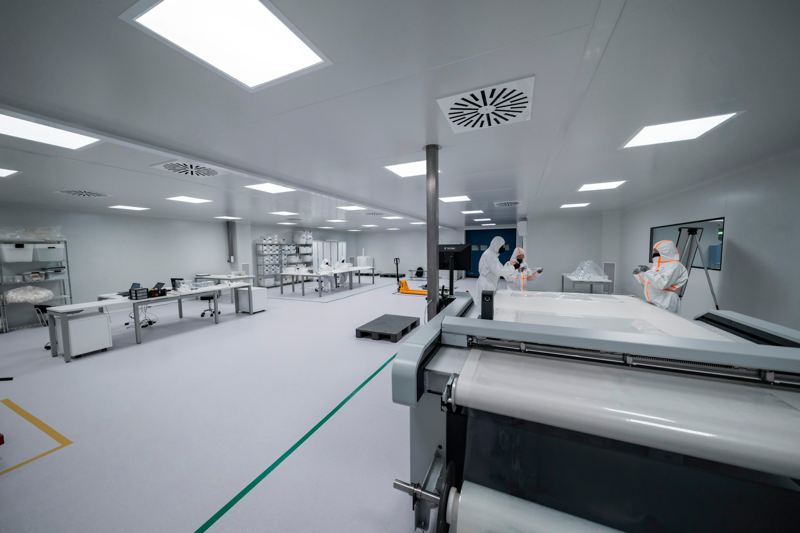
Siemens Healthineers has opened a €100 million semiconductor fabrication plant in Forchheim, Germany, dedicated to cadmium telluride detector production for photon-counting computed tomography systems.
The Photon-counting Sensor Fab gives the company a second industrial base for the semiconductor material used in its photon-counting CT detectors. Existing production in Japan is approaching its capacity limits, while the German operation places crystal growth and sensor manufacture alongside Siemens Healthineers’ established CT development and production activities in Forchheim.
The facility provides approximately 9,500m² of usable floor space and will create more than 100 jobs. Construction began in 2023, with the completed building and technical equipment representing an investment of around €100 million.
Production begins well before conventional electronic assembly. High-purity cadmium and tellurium are processed into seed and polycrystals before controlled crystal growth, with the two elements bonding at around 1,100°C. Siemens Healthineers says it takes approximately ten weeks for the cadmium-tellurium compound to form a single crystal.
The resulting material is cut and polished with submillimetre precision before a pixel structure is applied lithographically in a cleanroom. The completed semiconductor sensors then enter the company’s CT manufacturing process, where they are integrated into photon-counting scanners.
Uwe Rückl, head of CT Detectors & Crystals at Siemens Healthineers, said: “We do not want to rely on a single-site strategy in Japan.”
Photon-counting CT uses a different detector chain from conventional energy-integrating systems. Instead of first converting incoming X-rays into visible light through a scintillator, the CdTe semiconductor directly converts individual X-ray photons into electrical signals while retaining information about their energy.
That architecture can improve spatial resolution and provide spectral information while potentially reducing radiation dose, but it shifts a substantial part of the engineering challenge into semiconductor materials and detector manufacture. Crystal purity, defect density, wafer preparation, lithographic accuracy, and pixel consistency all affect the performance of the finished imaging system.
The long crystal-growth cycle also makes manufacturing yield particularly important. A defect discovered late in a process measured in weeks carries a different production penalty from one found during a short electronics assembly operation. Adding another qualified manufacturing site therefore provides capacity while reducing reliance on a single production location for a specialised detector material.
The Forchheim site already builds Naeotom Alpha, Siemens Healthineers’ first photon-counting CT scanner, launched in 2021. The original factory announcement said demand had increased substantially after launch, making local detector capacity part of the company’s attempt to shorten production times and reduce supply bottlenecks.
Siemens Healthineers has also built dedicated environmental controls into the fab. A single-digit million-euro investment has been made in air-emission and wastewater-treatment equipment for cadmium and tellurium processing, while waste heat from production is reused for building heating.
A 170kWp rooftop photovoltaic installation supplies renewable electricity, and the building has achieved LEED Platinum certification. Those measures sit alongside the more specialised process infrastructure required for crystal growth, wafer handling, lithography, and hazardous-material control.
The Forchheim investment has expanded since it was first announced in 2023, when Siemens Healthineers put the planned spend at €80 million. The completed project is now valued at approximately €100 million, reflecting the scale of the finished manufacturing and treatment infrastructure.
More importantly for detector supply, the site gives Siemens Healthineers a European production route for a semiconductor technology that is becoming central to its CT portfolio. The company can now develop scanners and manufacture the CdTe sensors that enable photon-counting operation at the same German location, while retaining its established production capability in Japan.
