IN Brief:
- Semi-Conductor Laboratory has introduced DMIS, an indigenous manufacturing execution system for semiconductor production.
- Its modular architecture covers order booking, wafer-fabrication activity, and final packaging within one shop-floor management platform.
- The system adds production workflow, manufacturing data, and traceability capability to India’s wider semiconductor manufacturing programme.
Semi-Conductor Laboratory has launched an indigenous manufacturing execution system for semiconductor production, adding a locally developed software layer for managing activity from order entry through wafer fabrication and final packaging.
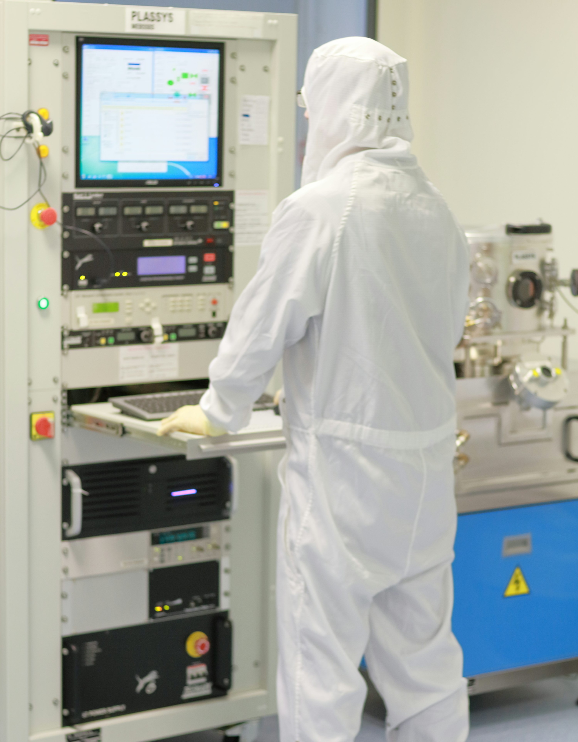
The Device Manufacturing Integrated System, or DMIS, was introduced during SEMICON India 2026 as a modular platform for fab automation. Government information describes it as a plug-and-play manufacturing execution system intended to improve control of wafer-fabrication activity while linking successive stages of semiconductor production through one operational framework.
A manufacturing execution system sits close to the production floor, unlike enterprise software used mainly for purchasing, finance, or corporate planning. It tracks work in progress, routes material through process steps, records equipment and lot status, manages recipes and production rules, and provides traceability when a wafer may pass through hundreds of tightly controlled operations before test and packaging.
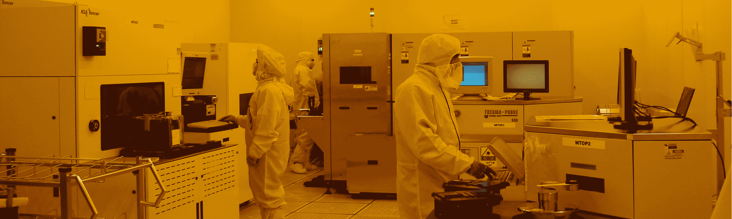
That role is particularly demanding in semiconductor manufacturing. A production lot moves repeatedly between deposition, lithography, etch, cleaning, implantation, metrology, and inspection stages, often revisiting related equipment groups several times. Process conditions, material genealogy, hold decisions, and equipment state all have to be associated with the correct lot and operation.
SCL says DMIS extends from order booking into wafer fabrication and final packaging, making it broader than a tool-monitoring application or isolated production dashboard. Public launch information does not yet disclose the underlying database architecture, equipment-interface standards, dispatch rules, cybersecurity model, or integration points with existing fab automation software.
The modular design is relevant because semiconductor factories rarely replace operational software as one monolithic project. Equipment generations, process modules, metrology systems, and back-end operations can expose different interfaces and data structures. A manufacturing execution platform has to connect established equipment while accommodating later tools and process changes without destabilising production control.
Traceability is another core requirement. Semiconductor failures can emerge late in assembly or field operation after an earlier process excursion, and manufacturers need to reconstruct the path of affected wafers through tools, recipes, materials, operators, measurements, and inspection decisions. The value of an MES therefore depends as much on the consistency of its manufacturing records as on the interface presented to production staff.
The software launch also broadens the scope of India’s semiconductor localisation programme. Much of the recent investment has focused on fabrication capacity, packaging plants, design programmes, equipment, and process materials. Production scheduling, manufacturing data, equipment integration, and quality traceability form another part of the same operating stack.
Recent front-end and packaging agreements around Tata Electronics illustrate the hardware and manufacturing-capacity side of that build-out. DMIS addresses the informatics layer required to coordinate semiconductor production once tools, processes, and material flows are in place.
SCL occupies an unusual position in that ecosystem. The Mohali organisation combines semiconductor fabrication with research, technology development, and support for domestic chip programmes, giving it a production environment in which manufacturing software can be developed against real process requirements rather than treated solely as an enterprise IT project.
Public information does not yet indicate whether DMIS will remain an SCL-specific system, be offered to other domestic semiconductor facilities, or form the basis of a wider commercial or government-supported platform. Details on supported equipment protocols, deployment scale, failover, data retention, and production qualification will matter if the system is extended beyond its originating fab.
A fab cannot be run simply by installing process tools in sequence. Those tools have to be orchestrated around lots, recipes, quality limits, maintenance events, engineering holds, and delivery schedules, with enough data integrity to support both process control and later fault analysis.
DMIS adds that operational layer to India’s domestic semiconductor effort. Its next useful milestones will be production deployment, the range of equipment and interfaces supported, and evidence that the system can manage continuous fab workflow without compromising traceability or uptime.