IN Brief:
- Infineon and Wolfspeed have signed a multi-year supply agreement for 200mm silicon carbide wafers.
- The arrangement builds on more than 20 years of cooperation involving 150mm substrate supply.
- The agreement supports Infineon's manufacturing transition, with contracted volumes and financial terms undisclosed.
Infineon Technologies and Wolfspeed have signed a multi-year agreement for 200mm silicon carbide wafers, extending an established supply relationship as Infineon converts more of its power semiconductor manufacturing from 150mm substrates. Announced on 15 October, the agreement supports the German manufacturer’s transition to larger wafers while providing an additional source of material for its silicon carbide production programme.
The companies have worked together for more than 20 years, with their existing arrangement covering 150mm silicon carbide substrates. Wolfspeed describes the latest agreement as an expansion and extension that adds 200mm supply, while Infineon characterises it as supporting the transition from 150mm to 200mm manufacturing. Neither announcement specifies the duration of any overlap between the two substrate formats, the quantity of wafers covered or the financial value of the contract.
Infineon has been developing 200mm silicon carbide manufacturing at its production sites in Villach, Austria, and Kulim, Malaysia. The company has already introduced commercial devices produced using larger-diameter substrates, and the latest agreement contributes to a wider sourcing strategy intended to support that manufacturing transition. It does not represent the opening of a new fabrication facility or the first production of 200mm silicon carbide devices.
Silicon carbide is a wide-bandgap semiconductor material used in power devices operating at high voltages, switching frequencies and temperatures. Its electrical characteristics can allow suitable converters to operate with lower losses than comparable silicon-based designs, particularly where conventional devices encounter limitations associated with voltage blocking, switching behaviour or thermal performance.
Those characteristics have encouraged the use of silicon carbide MOSFETs and diodes in electric vehicle traction inverters, charging systems, solar inverters, battery storage converters and industrial power electronics. Data centre power infrastructure is another developing application, particularly where equipment designers are seeking higher conversion efficiency and greater power density. The achievable improvements depend on the complete circuit architecture, including gate drive, passive components, cooling and operating conditions.
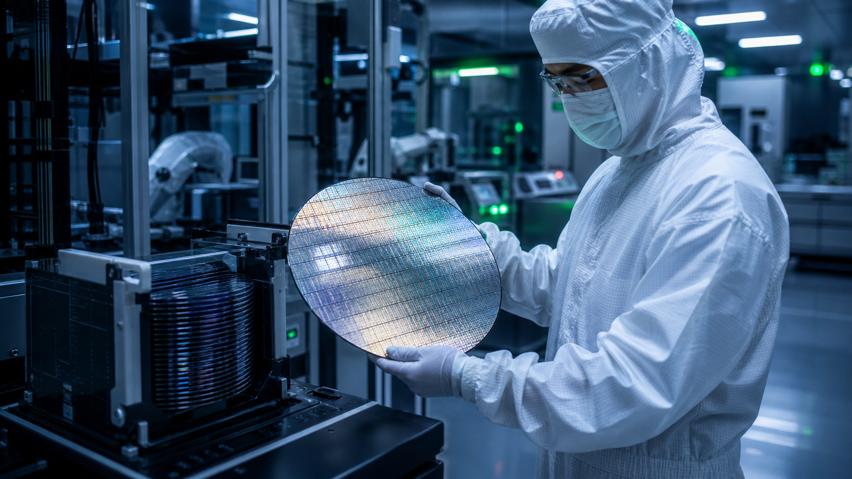
The move to 200mm substrates addresses a different part of the manufacturing process. Increasing the wafer diameter from 150mm to 200mm raises its nominal surface area by approximately 78%, creating the potential to accommodate more semiconductor devices during fabrication. The actual increase in usable die depends on their dimensions, spacing, wafer edge exclusions, defect distribution and processing yield, so the greater surface area cannot be translated directly into an equivalent increase in finished output.
Silicon carbide substrates also present manufacturing challenges that differ from those encountered with conventional silicon wafers. High-quality crystals must be grown, sliced and processed before an epitaxial semiconductor layer is deposited onto the wafer surface. Crystal defects, surface quality, wafer bow and variations in thickness can affect subsequent fabrication processes and the electrical behaviour of the finished devices.
Producing larger substrates introduces tighter requirements for process consistency across the wafer. Equipment used for epitaxy, deposition, lithography, etching, inspection and handling must accommodate the increased diameter while maintaining the required material and process characteristics. Changes in substrate size can also require additional qualification of manufacturing equipment, process recipes and device performance before commercial output reaches its intended scale.
Wolfspeed has separately been developing its 200mm materials portfolio. In September 2026, the company introduced a premium 200mm n-type silicon carbide substrate, highlighting improvements in material quality and wafer geometry. That was a product development distinct from the October supply agreement with Infineon. The latter concerns the commercial relationship between an established substrate manufacturer and a power semiconductor producer already pursuing larger-diameter fabrication.
Manufacturers must also consider how substrate quality affects downstream economics. A larger wafer may accommodate more devices, but defects introduced during crystal growth or subsequent processing can render individual die unusable. Consequently, consistent substrate supply and acceptable yield are closely connected. The commercial benefit of increasing wafer diameter depends on controlling these factors alongside the cost and throughput of fabrication equipment.
Infineon’s sourcing strategy includes several silicon carbide materials suppliers, reflecting the importance of securing qualified material during manufacturing expansion. Supplier diversity can reduce dependence on an individual production source, although different substrates must still satisfy the electrical, mechanical and quality requirements of the receiving fabrication process. Material from a new source cannot necessarily be substituted without appropriate qualification.
Alexander Gorski, chief operations officer at Infineon, identified the agreement as part of the company’s efforts to broaden its supply base for 200mm high-volume manufacturing. Robert Feurle, chief executive officer of Wolfspeed, described the extension as a continuation of their established relationship and support for Infineon’s longer-term material requirements. Neither company provided specific customer orders or device production forecasts arising from the agreement.
Wolfspeed also cited a Yole Group forecast estimating that the global silicon carbide power device market could grow from $3.4bn in 2024 to $11.1bn in 2031. The estimate represents a market projection rather than contracted semiconductor demand. Its relationship to the Infineon agreement remains indirect because the companies have not disclosed the volume of material they expect to exchange.
The immediate manufacturing development is a new commitment to supply 200mm substrates within a longstanding commercial relationship. The extent to which this supports increased device output will depend on wafer deliveries, qualification, fabrication yield and the pace of Infineon’s transition. The announcement establishes the supply arrangement but does not quantify those subsequent production outcomes.