IN Brief:
- Advanced electronics packaging increasingly combines wafer back-end work, die assembly, photonics, test, and qualification within one manufacturing chain.
- AEMtec adds chip-on-board, flip-chip, 3D integration, optoelectronic packaging, and cleanroom operations in Berlin and Dresden.
- Micross expects the transaction to close in the second half of 2026, subject to customary regulatory approvals.
Micross Components has entered into a definitive agreement to acquire German microelectronics manufacturer AEMtec, a transaction that would expand its European advanced packaging, optoelectronics, assembly, and test capability. Completion is expected during the second half of 2026, subject to customary regulatory approvals.
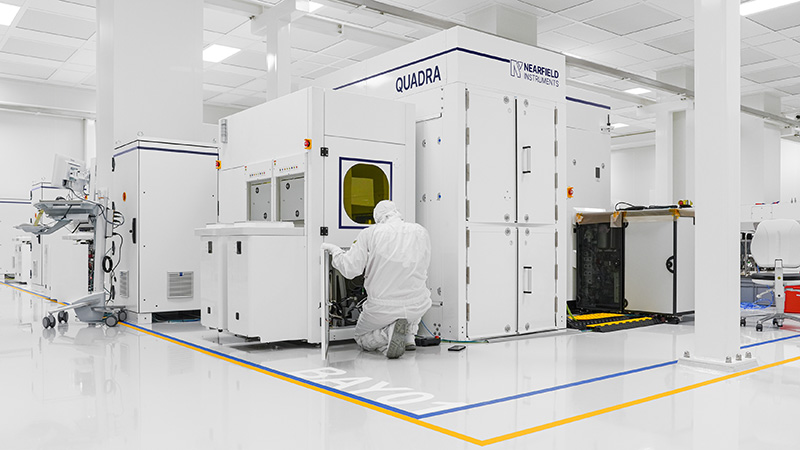
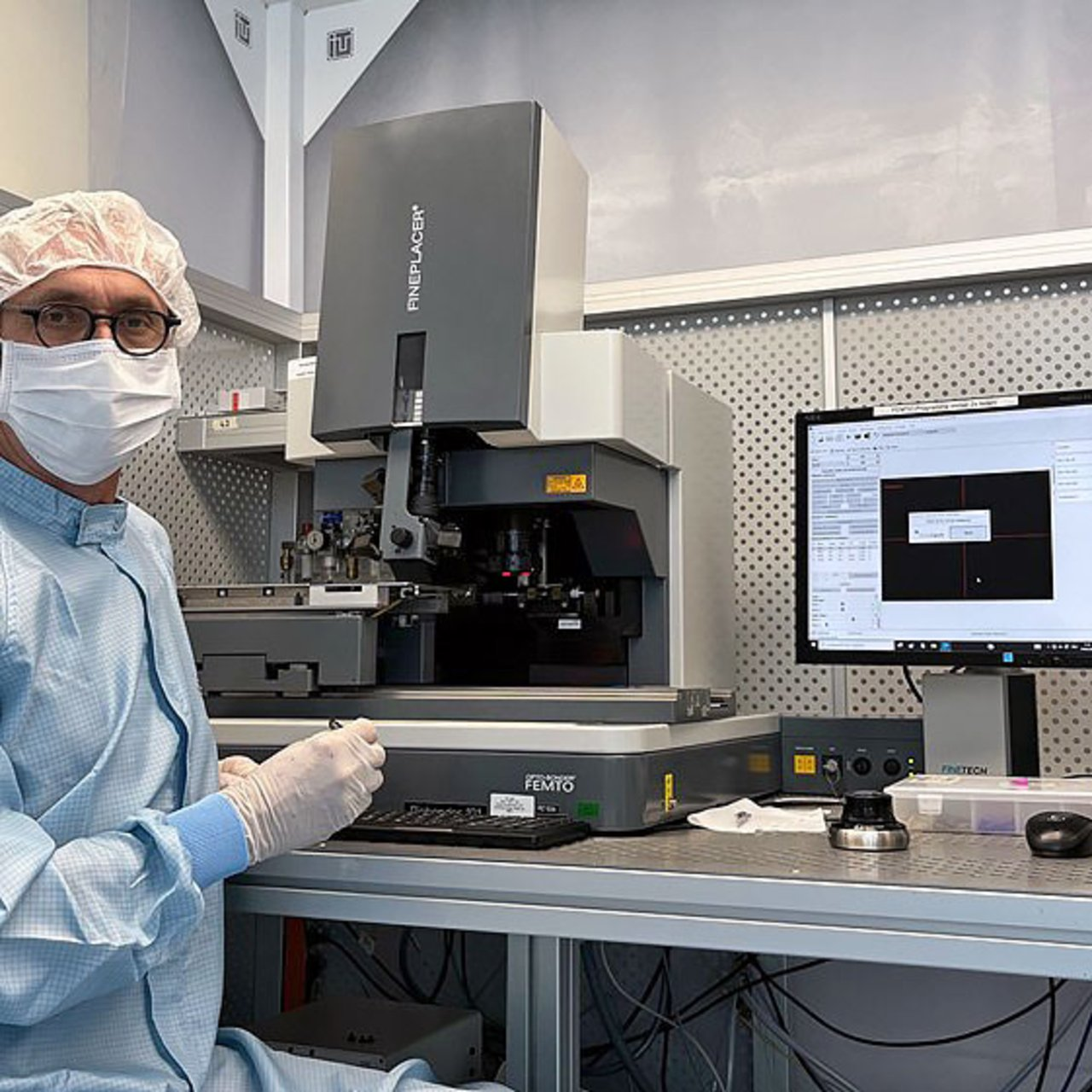
AEMtec is headquartered in Berlin and operates cleanroom facilities in Berlin and Dresden, alongside an operation in Boston. Its manufacturing portfolio includes wafer back-end services and wafer testing, chip-on-board assembly, flip-chip integration, 3D integration, optoelectronic packaging, prototyping, industrialisation, qualification, series production, and lifecycle support.
Micross already supplies high-reliability microelectronic products and services to aerospace, defence, space, medical, energy, communications, and industrial programmes. The proposed acquisition would establish a larger manufacturing and engineering presence in continental Europe while extending the range of assembly and packaging work that can be undertaken inside the group.
The industrial case goes beyond adding another production site. Advanced semiconductor systems increasingly derive performance from the way several dies, substrates, optical elements, passives, and interconnects are integrated rather than from one monolithic die alone. Chiplets, photonic modules, sensors, MEMS, and mixed-technology assemblies all push packaging deeper into the electrical and thermal design of the finished system.
AEMtec’s portfolio places it across several stages of that process. Wafer back-end services and test occur before devices are packaged, while chip-on-board and flip-chip techniques determine how bare die connect into the wider assembly. Three-dimensional integration adds another layer of interconnect density, and optoelectronic packaging introduces precise optical alignment alongside conventional electrical assembly.
Those functions become particularly demanding in high-reliability markets. Aerospace, defence, and medical electronics often require controlled materials, detailed traceability, environmental qualification, and long support periods. Production changes that might be routine in shorter-life commercial hardware can require extensive customer approval when a device or module forms part of a qualified programme.
Combining development and series production under the same manufacturing organisation can shorten some of the feedback loops that appear during industrialisation. A packaging concept that works across a handful of prototypes may encounter different problems when throughput increases: placement tolerances, bond yield, underfill behaviour, optical alignment, contamination control, automated inspection, and test coverage all become statistical production issues rather than isolated engineering tasks.
Failure analysis is similarly easier when process data can be traced through more of the manufacturing chain. A defect found during electrical, optical, or environmental qualification may originate in die preparation, interconnect, substrate design, assembly, encapsulation, or test. Dividing those stages between several suppliers adds another boundary each time engineers try to reconstruct the cause.
Geography is also part of the transaction. European semiconductor policy has concentrated heavily on wafer fabrication, but packaging, assembly, and test remain essential parts of any regional manufacturing chain. Localising those stages does not make the underlying semiconductor supply independent, although it can reduce the distance between design teams, customers, qualification activity, and final module production.
AEMtec’s optoelectronic capability is especially relevant as optical functions move into semiconductor packages. Co-packaged optics, sensing modules, and photonic integrated circuits require electrical and optical interfaces to be aligned and tested in one assembly, reducing the usefulness of treating photonics as a completely separate manufacturing discipline.
Integration will not happen simply because the transaction closes. Existing customer programmes may be qualified to particular facilities, tools, materials, or processes, and transferring production can require formal requalification. Retaining specialist engineers and process knowledge will also matter because advanced packaging capacity is defined as much by know-how and yield history as by the equipment listed on a cleanroom floor.
Financial terms have not been disclosed. Until closing, AEMtec remains a separate business, so the transaction should be treated as planned capacity rather than capacity already absorbed into Micross. If completed on schedule, however, it would give the company a broader European manufacturing base at a point when packaging and test are receiving rather more attention from customers who have discovered that processed silicon is only useful once someone can assemble and qualify it.