
IN Brief:
- Silicon Motherboard places functional dies on top of a silicon substrate and discrete passives beneath it.
- Wafer processing can also form transistor, resistor, and capacitor elements inside the substrate.
- Nisshinbo's window-comparator prototype reduced mounting footprint by about 80 per cent against its discrete reference design.
Nisshinbo Micro Devices has developed a three-dimensional packaging architecture that uses both sides of a silicon substrate to combine semiconductor dies, wafer-formed circuit elements, and discrete passive components inside one package. The company calls the technology Silicon Motherboard, or Si-MB, and reports that a window-comparator prototype reduced mounting footprint by about 80 per cent compared with its conventional discrete configuration.
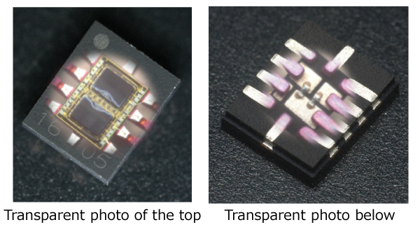
The structure places functional semiconductor chips on the upper surface of the silicon substrate. Transistors, resistors, and capacitor elements can also be formed within the substrate using wafer processing, while printed wiring on the underside provides mounting locations for additional passive components. The result is closer to a compact circuit assembly inside a semiconductor package than to a conventional single-die IC.
Nisshinbo is using the underside primarily to accommodate components that are inconvenient to realise within the same silicon process as the active circuitry. Its examples include capacitors above 1,000 pF, resistors below 1 Ω, and inductors. Those values are familiar at PCB level, but integrating them alongside analogue circuitry can become difficult when the active device package has already been reduced to only a few millimetres.
The prototype implements a window comparator with two comparator ICs mounted as functional chips. Resistive elements are formed in the silicon, and two chip resistors are attached to the printed wiring on the bottom surface. Nisshinbo says consolidating those elements into Si-MB reduced the occupied mounting area by around four-fifths compared with the equivalent discrete implementation.
The attraction for analogue design extends beyond raw area. Comparators, operational amplifiers, regulators, and sensor interfaces often rely on external resistor, capacitor, and inductor networks that determine gain, filtering, thresholds, compensation, or power integrity. Once those elements are brought into the same packaged assembly, their interconnects become shorter and the supplier can optimise more of the complete circuit rather than leaving every peripheral component to the PCB designer.
That integration also changes the design trade-off. A resistor or capacitor placed on the PCB can be changed relatively late in development, sourced from several vendors, or adjusted between product variants. A passive embedded within a packaged module is less accessible, so density has to be balanced against configurability, repairability, qualification effort, and the number of variants required to serve different customers.
Nisshinbo is trying to reduce another adoption barrier by retaining package outlines already used in mass-produced products. The company says Si-MB does not require a new external package shape, allowing customers to use existing placement equipment and established assembly processes. That is significant because a dense package delivers little manufacturing benefit if it forces a customer to add specialist board-level equipment merely to handle it.
Reliability will still have to be demonstrated at product level. Mounting active dies, wafer-formed elements, and discrete passives on different parts of the same silicon structure introduces mechanical and thermal interfaces that must survive assembly, temperature cycling, and operating stress. Industrial and automotive applications add longer service lives and harsher environmental conditions than a simple laboratory prototype, so the eventual package qualification will matter as much as the dimensional reduction.
The technology also sits in a different design space from the high-end chiplet platforms used to assemble large digital processors. Nisshinbo is targeting analogue functions and their peripheral components, where board area can be consumed by the network around the IC rather than the silicon die itself. The company sees that as a route from supplying individual analogue ICs towards more complete system solutions.
Whether Si-MB becomes useful at scale will therefore depend on the circuits selected for integration. Functions with stable external networks, demanding area constraints, and high production volumes are more obvious candidates than designs that rely on frequent component changes. The window-comparator demonstrator proves that Nisshinbo can place several familiar circuit elements into the same package; the next evidence will come from production devices showing that the area saving survives cost, reliability, and manufacturing requirements.
