IN Brief:
- Gen4 QSiC devices include 750V and 1,200V MOSFETs with specified on-resistance of 9mΩ and 11mΩ respectively.
- SemiQ reports a 21% resistance reduction for the 1,200V device against its third-generation equivalent, while retaining a 5 × 5mm die.
- Packaged TO-247-4L and bare-die versions are available, with wafer-level gate-oxide screening and avalanche testing included in production.
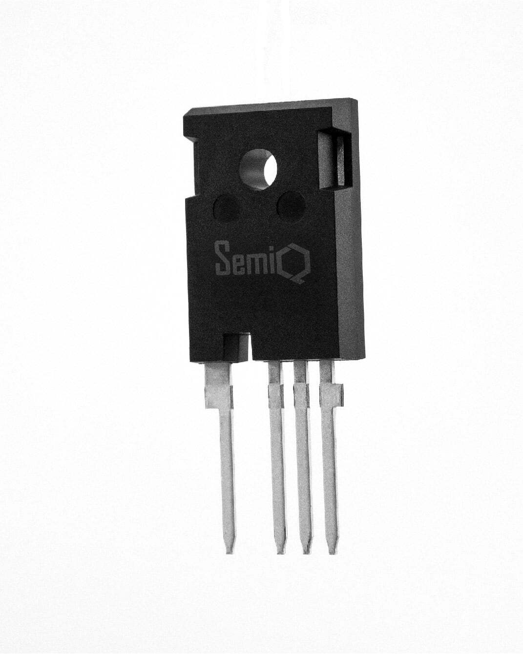
SemiQ has introduced fourth-generation silicon carbide MOSFETs for high-voltage power conversion, adding 750V and 1,200V devices with lower specified on-resistance and revised semiconductor cell structures. The Gen4 QSiC range is available in four-pin TO-247-4L packages and bare-die configurations, targeting applications including industrial drives, charging infrastructure and renewable energy converters.
The 1,200V GP4T011A120H has a specified on-resistance of 11mΩ, compared with 14mΩ for the manufacturer’s third-generation reference device. SemiQ reports a reduction of approximately 21% while retaining the same 5 × 5mm semiconductor die dimensions.
The new 750V device, GP4T009A075H, provides a lower-voltage option with specified on-resistance of 9mΩ. The company has introduced this voltage class within its fourth-generation range to address converter architectures that do not require the higher 1,200V blocking capability.
Voltage rating determines the maximum drain-to-source voltage a MOSFET is designed to withstand under its specified operating conditions. The selected rating must accommodate the converter’s DC bus voltage and transient stresses, with appropriate design margin for switching overshoot and other conditions that can occur during operation.
On-resistance determines a significant part of the power dissipated while a MOSFET is conducting. Resistive conduction loss increases with the square of current, so even a relatively small reduction in resistance can affect heat generation when current is high.
The benefit is not fixed across every operating condition. Silicon carbide MOSFET on-resistance changes with junction temperature, while actual current waveforms, conduction intervals and thermal conditions influence the losses in a completed power stage.
SemiQ attributes its fourth-generation resistance improvement to a redesigned cell topology, including a 36% reduction in cell pitch and modifications to the junction field-effect transistor region and P-well implantation. These changes alter the conducting structure within the die and the balance between current capability and voltage blocking.
The company reports a 23% reduction in specific on-resistance compared with earlier generations. Specific on-resistance relates resistance to semiconductor area, allowing performance comparisons that account for differences in die dimensions rather than relying only on the resistance of a finished device.
Maintaining a 5 × 5mm die while reducing the resistance of the 1,200V product indicates an improvement in the conducting characteristics of the semiconductor structure. The impact on production cost and manufacturing yield cannot be established from the die dimensions alone.
Switching behaviour is another focus of the redesign. During transitions between conducting and blocking states, voltage and current overlap for a finite interval, producing energy loss. These losses increase with switching frequency when the energy dissipated per transition remains comparable.
SemiQ reports that its fourth-generation 1,200V device reduces total switching energy by more than 11% against the preceding design. The comparative figures in the product announcement contain inconsistent absolute units, so the published percentage should be treated as a manufacturer claim until the relevant datasheet measurements and test conditions are independently reconciled.
The total switching loss of a converter also depends on gate resistance, gate-drive voltage, switching current, DC bus voltage, parasitic inductance and the thermal behaviour of the devices. A semiconductor improvement can reduce losses under comparable conditions without guaranteeing an equivalent reduction in total converter power consumption.
The four-pin TO-247-4L package provides a separate source connection for the gate-drive return path. This arrangement helps reduce the effect of common-source inductance, which can interfere with control of the gate-to-source voltage as current changes rapidly through the main power terminals.
Separating the gate-drive return can support more predictable switching transitions, particularly in high-current circuits. PCB geometry, gate-loop layout, decoupling and the wider power-stage arrangement remain important because additional parasitic inductance can produce voltage overshoot and electromagnetic interference.
Both voltage classes are also supplied as bare dies. These versions allow power-module designers to select their own die-attachment, interconnection and thermal arrangements instead of relying on the standard discrete package.
Bare-die integration introduces further manufacturing requirements. Die bonding, electrical isolation, current distribution and thermal cycling must be qualified within the finished module, particularly where several devices are connected in parallel or subjected to repetitive high-power operation.
SemiQ states that the new devices undergo wafer-level gate-oxide burn-in screening at voltages exceeding 1,400V for the 1,200V devices and 800V for the 750V variants. It also reports avalanche testing to an energy level of 800mJ for both voltage classes.
These production tests provide information about semiconductor quality and response to defined electrical stresses. They do not establish that a finished converter can tolerate unlimited avalanche events or operate outside the device’s published safe operating conditions.
The new devices are available in four variants, pairing the GP4T009A075H and GP4T011A120H packaged products with corresponding GP4T009A075X and GP4T011A120X bare dies. SemiQ will also demonstrate the range through distributor Alfatec at electronica 2026, following its commercial introduction.