IN Brief:
- Europe currently lacks domestic commercial production of semi-insulating SiC substrates used beneath GaN RF and high-power devices.
- GaN epitaxy has been grown on TekSiC wafers, enabling Chalmers University of Technology to begin RF and power HEMT processing.
- Customer validation wafers are planned for mid-2027, followed by industrialisation and production scale-up from the end of 2027.
TekSiC has reached a material-integration milestone in Sweden’s effort to establish a domestic semi-insulating silicon carbide supply chain, after GaN epitaxial layers were successfully grown on its SiC wafers. The result allows project partner Chalmers University of Technology to move the epiwafers into RF and power HEMT device processing.
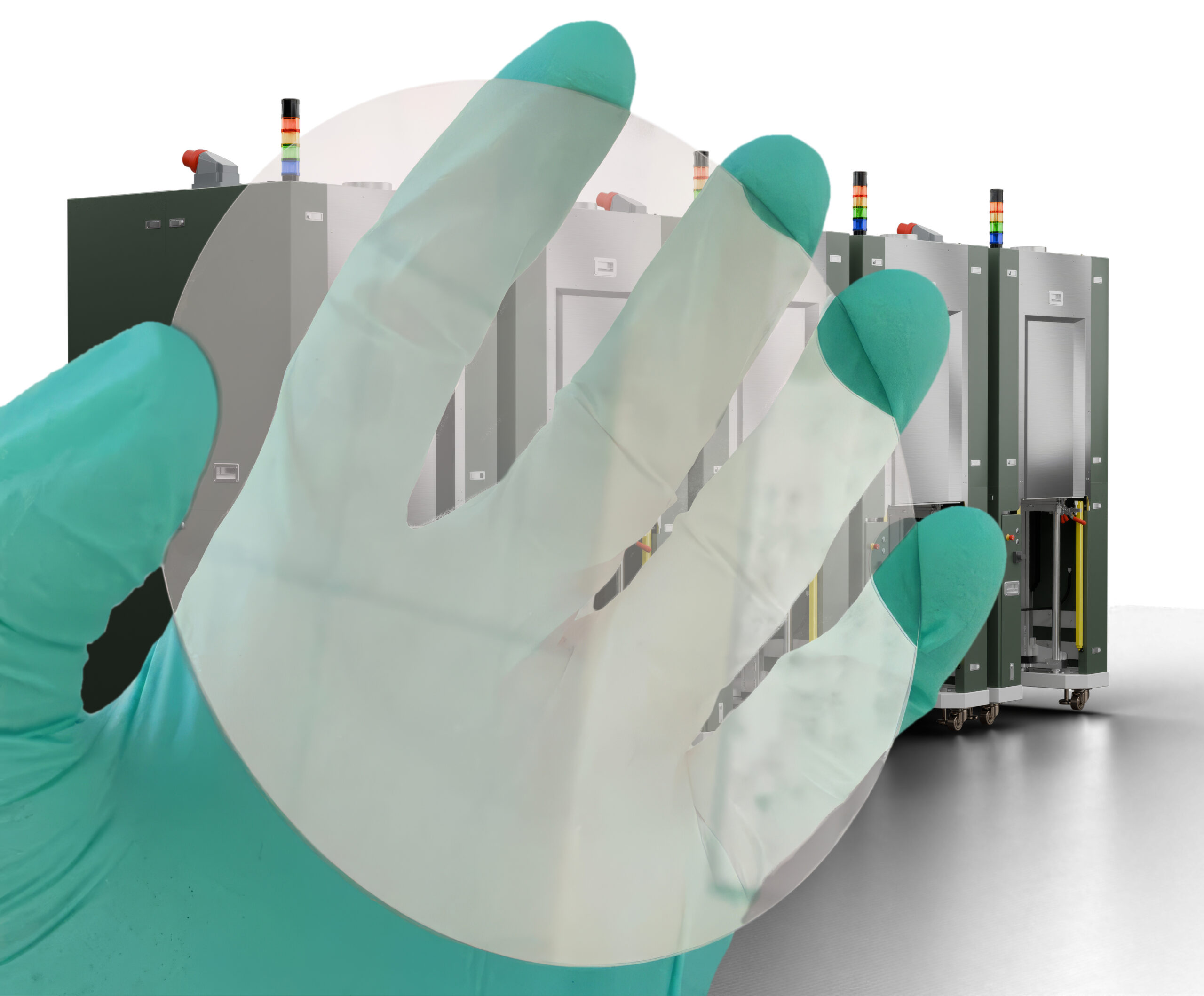
The Linköping company is developing semi-insulating SiC, a high-resistivity substrate used beneath GaN layers where high-frequency, high-power, low-noise operation is required. Initial development is centred on 100mm substrates, while TekSiC says the growth process is already prepared for a move to 150mm wafers.
According to the company, Europe currently lacks domestic commercial manufacturing capability for this class of substrate. Semi-insulating SiC is used beneath GaN HEMTs and RF power devices serving radar, satellite communications, electronic warfare, advanced sensing, and 5G or 6G infrastructure, placing substrate availability inside both a materials and supply chain problem.
The development sits inside the Swedish government-backed “Semiconductor, A Swedish Value Chain” programme, launched in March 2025 to demonstrate a domestic route from raw material to functioning devices. TekSiC is responsible for the SI-SiC substrate, SweGaN grows the GaN epitaxy, and Chalmers carries out RF and power HEMT development. Polar Light Technologies is also expected to use material from the programme for micro-LED work.
The latest milestone follows TekSiC’s earlier demonstration of high-resistivity material and the establishment of an in-house wafer pilot laboratory covering slicing, polishing, and characterisation. Bringing more of those steps together gives the company a shorter feedback loop between crystal growth and finished-wafer measurements, which is useful when defects introduced upstream can remain hidden until polishing, epitaxy, or device processing.
Crystal growth uses TekSiC’s own Xforge physical vapour transport equipment, with the company also developing proprietary AHM technology intended to improve crystal quality and yield while reducing wafer cost and process-related carbon emissions. Those claims will ultimately be tested by the uniformity, defect density, electrical behaviour, and production yield achieved as wafer diameter and output increase.
The Swedish programme is developing alongside a wider expansion of GaN-on-SiC capability in Linköping. SweGaN has raised $14m to expand GaN-on-SiC epiwafer capacity, with commercial orders spanning RF and power applications in defence, aerospace, telecommunications, and data centre equipment. TekSiC occupies the upstream layer of that stack, where the substrate determines how much of the finished material chain can be sourced within Europe.
Semi-insulating wafers are a more specialised product than conductive SiC substrates used in mainstream automotive power electronics. RF performance is sensitive to crystal defects, resistivity uniformity, thermal transport, and the behaviour of the GaN interface above the substrate, so qualification cycles can be lengthy and customer-specific. A domestic source therefore has to demonstrate more than the ability to grow a crystal with the correct nominal resistivity.
Scaling from 100mm development wafers to 150mm will add another manufacturing test. Larger crystals have to maintain quality across a wider usable area, while slicing, polishing, bow, thickness variation, and edge losses all influence how much saleable wafer emerges from each boule. The economics become increasingly dependent on repeatable yield rather than isolated material measurements.
TekSiC plans to make wafers available for customer validation by mid-2027, with industrialisation and production scale-up expected to begin towards the end of that year. A second investment round is also planned for mid-2027 to support that industrial phase, following an initial round led by Turbine Capital.
The next technical checkpoint is the demonstration of functioning RF and power HEMT structures made on TekSiC substrates. Device processing will expose defects, interface problems, and uniformity issues that resistivity measurements alone cannot reveal. Europe has no shortage of semiconductor capacity ambitions; this programme is now at the more useful stage where the material has to survive epitaxy, fabrication, and customer qualification.