
IN Brief:
- La Luce Cristallina has released a beta 200mm BaTiO₃ wafer for customer evaluation.
- The platform targets low-voltage electro-optic modulators for telecoms, datacoms, AI data centres, and quantum photonics.
- Co-packaged optics are increasing demand for materials that reduce switching energy and integrate with silicon manufacturing.
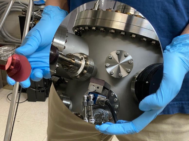
La Luce Cristallina has made a beta version of its 200mm barium titanate wafer available to customers for evaluation in advanced electro-optic modulator designs.
The wafer targets telecommunications, data communications, AI-scale data centre infrastructure, supercomputing, quantum photonics, and other high-capacity optical applications. The company’s BaTiO₃ platform is designed for ultra-low-voltage operation and integration into standard CMOS silicon manufacturing processes.
Barium titanate offers a high Pockels coefficient, the property that describes the strength of a material’s linear electro-optic effect. In an electro-optic modulator, that effect allows an applied electric field to change the refractive index of the material, enabling optical signals to be switched or modulated.
The company’s bulk single-crystal BaTiO₃ has been reported with a coefficient of around 1,300pm/V. That level of electro-optic performance makes the material attractive for low-loss, high-speed switching where energy consumption, bandwidth, and footprint are becoming increasingly difficult constraints.
Availability of a beta 200mm wafer moves the platform closer to the manufacturing scale needed for silicon photonics integration. Smaller demonstrations can prove physical performance, but data centre and telecoms adoption depends on repeatability, process compatibility, yield, inspection, packaging, and integration with existing wafer flows.
Co-packaged optics are gaining urgency as AI infrastructure pushes electrical interconnects closer to practical limits. Accelerator clusters need high-bandwidth, low-latency links, while the energy consumed moving data between processors, memory, switches, and optical interfaces has become a major design constraint. Lower-voltage modulators can reduce power consumption inside the optical link budget.
Material selection is central because silicon photonics brings both scale and limitations. Silicon offers mature processing, manufacturing reach, and integration advantages, but electro-optic performance often depends on materials added to or combined with the silicon platform. BaTiO₃ is one route among several being explored to improve modulation efficiency without abandoning silicon-compatible production.
Process innovation around atomic pitch splitting shows how future semiconductor and photonics performance depends on more than transistor scaling alone. Materials, patterning, packaging, and optical integration are all becoming part of the performance stack.
Packaging capacity will also influence adoption. The move to strengthen European chip packaging through Tessalia points to a wider need for advanced assembly, alignment, thermal management, and heterogeneous integration. Optical I/O and co-packaged optics place especially high demands on these downstream processes.
The beta wafer phase will test more than headline material properties. Customers will evaluate loss, uniformity, reliability, process windows, wafer handling, interface quality, and compatibility with foundry flows across real modulator designs. Wafer-scale electro-optic performance has to survive the practical demands of silicon photonics manufacturing.
La Luce Cristallina’s 200mm BaTiO₃ wafer gives photonics developers another route to lower switching energy as AI infrastructure forces a rethink of interconnect design. Customer validation will decide whether the material can move from promising electro-optic performance into qualified photonic systems and volume manufacturing pathways.

