IN Brief:
- IHP has released an open-source assembly design kit for heterogeneous chiplet systems.
- The Open ADK links 2.5D assembly design with a route to fabrication.
- The release strengthens Europe’s open semiconductor design infrastructure.
IHP – Leibniz Institute for High Performance Microelectronics has released an open-source Assembly Design Kit for heterogeneous chiplet systems, giving designers a more direct route from multi-die packaging concepts to manufacturable hardware.
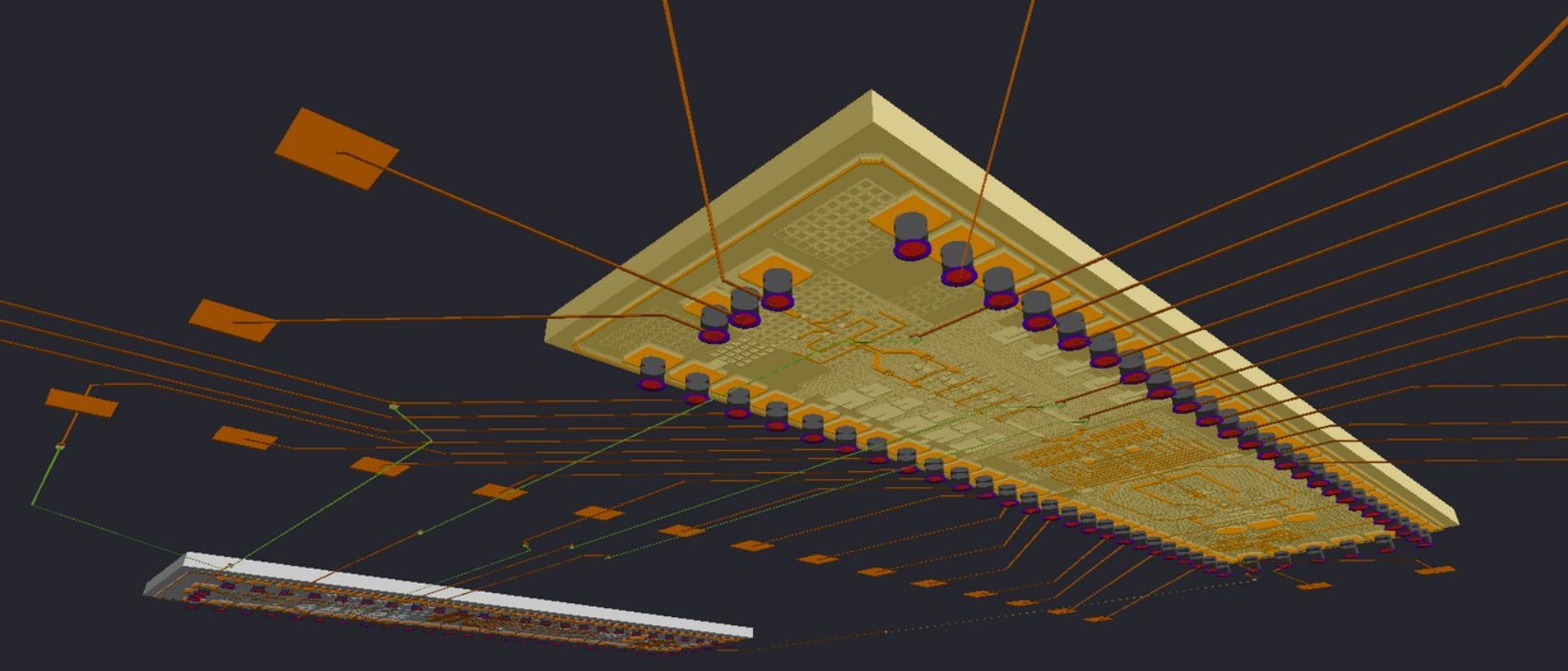
Developed for 2.5D assembly and interposer-based design, the IHP Open ADK extends open semiconductor design activity beyond individual integrated circuits and into the physical integration layer that increasingly defines advanced electronics. The release builds on IHP’s earlier open-source process design kit work for its SG13G2 130nm SiGe BiCMOS technology, adding another layer of design infrastructure for projects that need to move beyond single-die layouts.
Chiplet architectures have become central to discussions around processors, RF systems, photonics, AI accelerators, automotive electronics, and advanced sensing, although the route from concept to buildable hardware remains difficult. Verified rules, assembly constraints, interposer data, die placement information, and a fabrication path all have to be available before a design can progress from architectural intent to a working prototype.
Packaging now carries a growing share of the electrical design burden. Signal integrity, power distribution, thermal paths, interconnect density, die-to-die interfaces, test access, and yield are all shaped by package-level decisions, making the assembly environment part of the design problem rather than a late-stage manufacturing detail. Open access to that environment gives universities, research groups, startups, and collaborative semiconductor projects a more practical way to explore heterogeneous integration.
The same shift is visible in the semiconductor and electronic systems activity around TechWorks and S2S26, where the emphasis is moving from isolated process capability toward wider design, packaging, systems, and commercial collaboration. Open design infrastructure does not replace the need for foundry relationships, packaging expertise, or commercial EDA tools, but it lowers the barrier to early experimentation and shared development.
Multi-die systems are also forcing engineers to think across a broader technology stack. A chiplet concept may combine analogue, RF, digital, memory, sensor, photonic, or power-management functions, each with different electrical and thermal requirements. The assembly substrate then becomes the point where those requirements either become a practical system or a collection of incompatible building blocks.
Commercial packaging and EDA flows will remain essential for high-volume industrial programmes, particularly where qualification, reliability, and supply-chain control are central. IHP’s Open ADK instead gives earlier-stage projects a route into package-aware design before they reach that level of investment. It should make it easier to teach, test, and iterate designs that reflect real assembly constraints rather than idealised diagrams.
As chiplet development moves beyond the largest semiconductor companies, that access becomes more important. Smaller design groups need credible design data before they can contribute specialist die, test structures, RF blocks, mixed-signal interfaces, or research IP to more complex systems. Without that foundation, chiplets risk becoming a closed architecture dominated by companies with the budget to absorb the integration cost.
IHP’s release is infrastructure rather than spectacle, but that is precisely where much of Europe’s semiconductor challenge now sits. More open process and assembly data gives designers a clearer path from circuit concept to packaged prototype, and it places manufacturable heterogeneous integration within reach of a wider engineering base.