
IN Brief:
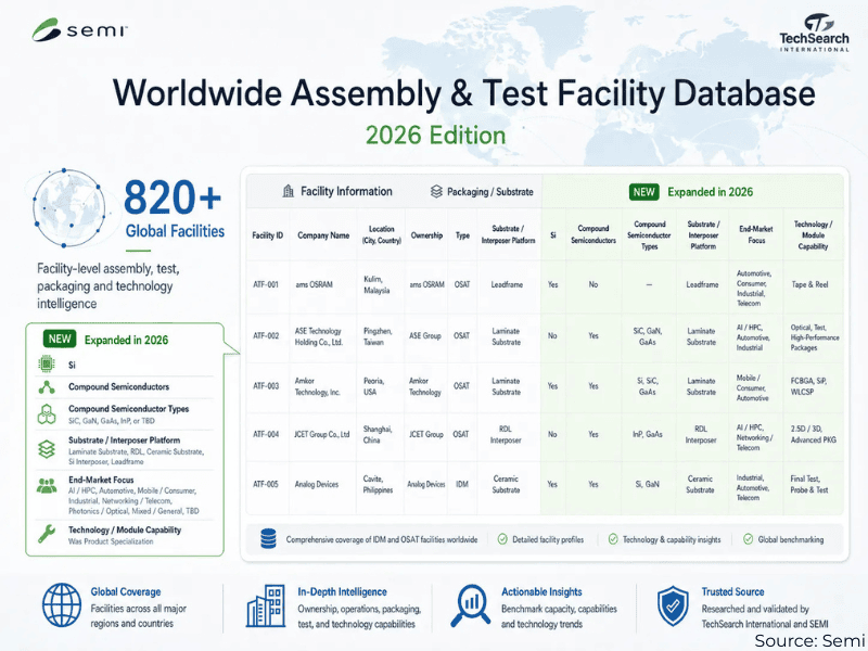
- SEMI and TechSearch International have released the 2026 Worldwide Assembly & Test Facility Database.
- The database now covers more than 820 semiconductor backend facilities worldwide.
- New fields give clearer visibility into advanced packaging, compound semiconductors, AI infrastructure, and photonics capability.
SEMI and TechSearch International have released the 2026 edition of the Worldwide Assembly & Test Facility Database, expanding coverage to more than 820 semiconductor backend manufacturing facilities worldwide.
The latest edition increases the database from around 750 facilities in the previous version, with the largest additions coming from China and Taiwan. The expanded dataset covers assembly and test facilities operated by integrated device manufacturers and outsourced semiconductor assembly and test companies, giving a broader view of where backend capacity is located, what it supports, and how the sector is evolving.
Facility-level detail now covers advanced packaging, module assembly, test services, specialised manufacturing capability, ownership, location, operating status, automotive certification, and manufacturing history. New classifications also cover compound semiconductor capability, AI and high-performance computing target markets, photonics and optical applications, and substrate or interposer platforms including laminate substrates, redistribution layers, ceramic substrates, silicon interposers, and leadframes.
The expanded data shows how quickly backend manufacturing has moved into the strategic semiconductor discussion. More than 360 facilities in the database report compound semiconductor capabilities across silicon carbide, gallium nitride, gallium arsenide, and indium phosphide. More than 170 identify AI and high-performance computing as target markets, while more than 70 support photonics and optical applications.
Advanced packaging has moved from a manufacturing support function into a system-level constraint. AI accelerators, high-bandwidth memory, chiplets, silicon interposers, co-packaged optics, and dense multi-die assemblies all depend on backend capacity that can handle tighter interconnects, larger package formats, thermal complexity, yield control, and high-volume test.
The same shift is visible across recent European semiconductor activity. IHP’s open assembly design kit for heterogeneous chiplet systems added a design route for advanced packaging research, while MKS’ Atotech expansion strengthened equipment capacity for semiconductor, advanced packaging, and PCB production. At the high-reliability end of the market, the Thales, Radiall, and Foxconn Tessalia venture is aimed at European system-in-package capacity.
The database update gives that wider trend a clearer manufacturing map. Wafer fabrication remains central to semiconductor strategy, but supply can no longer be understood by fab location alone. Assembly route, packaging technology, test capability, substrate availability, and regional concentration can all determine whether a chip becomes a qualified component in time for production.
AI infrastructure is sharpening the constraint. Processor scaling is being paired with memory proximity, packaging bandwidth, dense interconnect, and optical I/O. A leading-edge compute die can still be limited by package availability, substrate capacity, thermal design, test bottlenecks, or assembly yield. Backend visibility now influences sourcing, investment, qualification, and design planning.
Automotive, industrial, medical, defence, and communications markets face their own version of the same problem. Qualification discipline, long-term availability, traceability, and predictable change control are central requirements. A packaging change can affect electrical behaviour, thermal performance, reliability data, and mechanical fit, placing backend manufacturing inside product assurance rather than after it.
SEMI’s expanded database will not add capacity on its own, but it improves visibility into a layer of the supply chain now carrying more technical and commercial risk. As advanced electronics becomes more package-defined, the ability to map assembly and test capability will shape design planning as much as procurement strategy.

