
IN Brief:
- The reference circuit occupies 12.87mm² and uses the converter IC, one inductor, and three capacitors.
- The BD83070GWL provides up to 97% efficiency with quiescent current of 2.8µA.
- Published layout and bill-of-materials resources provide a direct route from evaluation into compact product design.
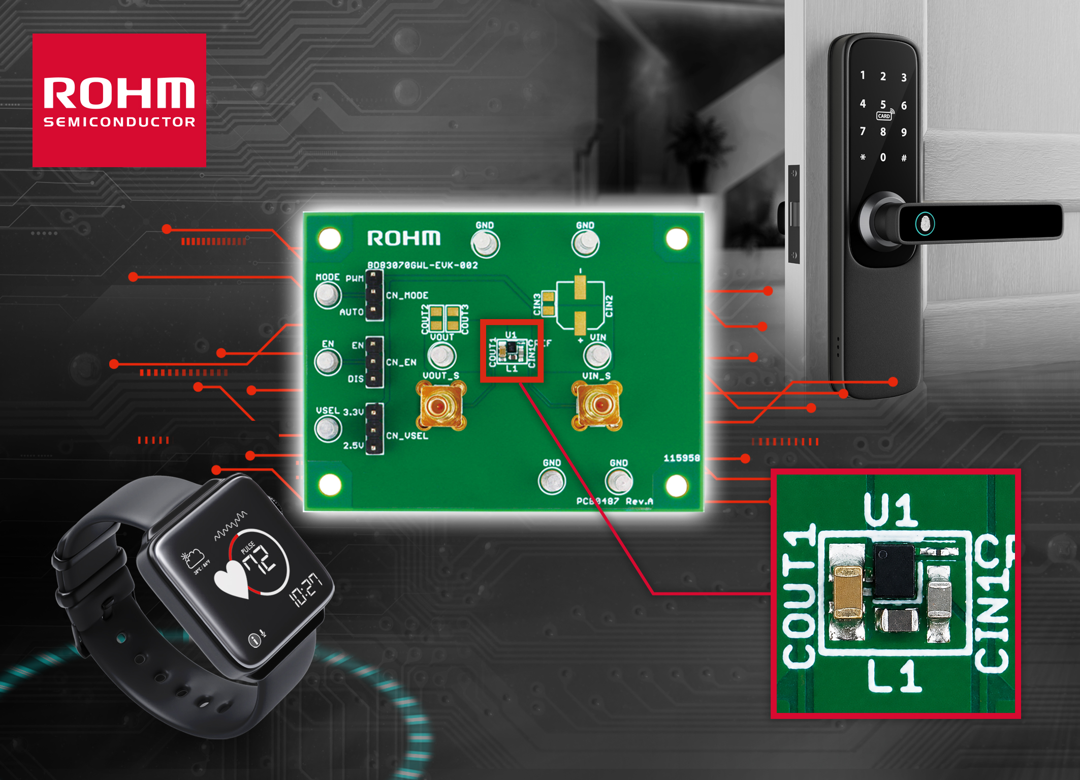
ROHM has introduced the BD83070GWL-EVK-002 evaluation board, demonstrating an ultra-compact buck-boost converter circuit for wearables, portable equipment, wireless sensors, and products powered from small batteries.
Built around the BD83070GWL converter IC, the power stage uses five principal components: the IC, one inductor, and three capacitors. Its mounting area measures 3.3mm by 3.9mm, occupying 12.87mm² on the printed-circuit board.
Conversion efficiency reaches 97% under specified conditions, while quiescent current is 2.8µA. The synchronous buck-boost architecture maintains a regulated output when the battery voltage moves above or below the required system rail during discharge.
Input voltage extends from 2V to 5.5V, and the device can provide a selectable 2.5V or 3.3V output. Output current reaches 1A when the input voltage and operating conditions meet the required limits, while automatic pulse-frequency and pulse-width modulation supports efficient operation across changing loads.
Alongside the evaluation hardware, ROHM has published the circuit pattern, schematic, component list, and board-layout information. These resources allow the demonstrated power stage to serve as a production reference rather than only a means of confirming basic converter operation.
Potential applications include smart watches, biometric sensors, smart rings, wireless earbuds, digital keys, Bluetooth Low Energy products, AI sensor nodes, smart locks, compact drones, and portable medical or personal-care equipment.
Compact layouts concentrate electrical and thermal demands
Buck-boost regulation suits single-cell products because the battery voltage can cross the required system rail during its discharge cycle. A nominal lithium-ion cell may begin above 3.3V and fall below it before reaching its discharge limit, leaving a buck-only converter unable to regulate the rail throughout the usable capacity.
Combining buck and boost operation avoids handing the supply between separate converters, although the topology can require more switching elements and a more involved control scheme. Reducing the external circuit to one inductor and three capacitors limits the board area consumed by the power stage, where the battery, antenna, sensors, display, and mechanical features are already competing for space.
Published layout information is particularly useful because switching-converter performance depends on current-loop geometry as well as the controller specification. Input and output capacitors require short, low-impedance connections, while the switching node must be contained to reduce ringing, electromagnetic emissions, and coupling into sensitive analogue or radio circuits.
Changes to the reference layout can alter ripple, stability, efficiency, and emissions even when the schematic remains identical. PCB layer count, ground structure, via placement, passive-component packages, and nearby circuitry all affect the electrical behaviour, so the reference pattern provides a starting point rather than a substitute for validation in the finished design.
Quiescent current becomes significant when the load remains asleep for most of its operating life. A converter that performs efficiently at hundreds of milliamperes can still consume a large part of the available energy while supplying a retention rail or dormant sensor, and the full budget must include divider currents, protection devices, monitoring circuits, and PCB leakage.
Peak efficiency also describes only one point within a broader operating range. A wearable or connected sensor may alternate between long periods at microampere load and brief radio or processor bursts, making the energy consumed across a complete operating cycle more useful than the maximum conversion figure.
Thermal behaviour can become limiting as the layout contracts because losses in the IC and inductor are concentrated within a small area. A sealed wearable or sensor housing may provide little copper or airflow for heat spreading, while minimum input voltage and maximum load usually produce the highest current.
Inductor saturation current, DC resistance, tolerance, and temperature rise therefore require attention alongside nominal inductance. A smaller component reduces mounting area but may increase copper loss or approach saturation during load transients, changing converter efficiency and stability.
Radios and processors also demand rapid transient response when leaving a low-power state. The output capacitors must supply the initial current while the control loop changes operating point, yet larger capacitors increase area, start-up time, and inrush current. Excessive voltage droop can reset the load before the converter reaches the required output.
The BD83070GWL-EVK-002 packages those compromises within a compact, documented implementation. Preserving its performance in production will depend on close control of current loops, passive selection, load behaviour, electromagnetic emissions, and temperature inside the final enclosure.

