IN Brief:
- Silicon Labs has opened a semiconductor design, testing, and validation laboratory at its Austin headquarters.
- A $23 million Texas Semiconductor Innovation Fund grant supported equipment for more advanced process-node development.
- The facility will support Series 3 and other secure, low-power wireless semiconductor platforms.
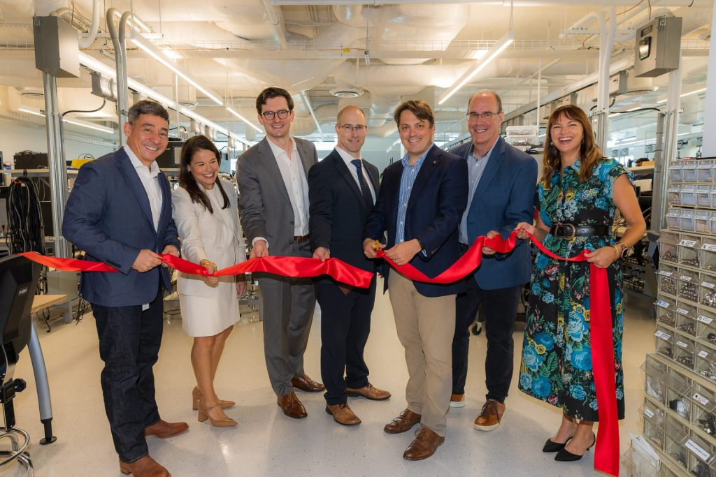
Silicon Labs has opened a semiconductor research and development laboratory at its Austin headquarters, adding chip-design, testing, and validation capability with support from a $23 million Texas Semiconductor Innovation Fund grant.
The facility forms part of the company’s Austin Innovation Center and will support development of low-power wireless semiconductors and connected-device platforms. Silicon Labs says the laboratory includes research, test, validation, and engineering equipment able to support work on more advanced wafer process technologies.
The Austin expansion is an R&D investment rather than a semiconductor fabrication project. Silicon Labs remains a fabless supplier, so commercial wafer production continues to be carried out by external manufacturing partners while design, characterisation, and product validation are handled internally.
The distinction determines where the new equipment contributes. Semiconductor designs have to be characterised across voltage, temperature, process variation, radio conditions, power states, and application scenarios before their published limits can be established with confidence.
More advanced process nodes can make that work increasingly demanding. Leakage, RF behaviour, analogue performance, operating margins, and device variability change as geometries shrink, while more functions are integrated into each die. Additional internal test capability can shorten the feedback loop between a design revision and measured silicon results.
The Texas Semiconductor Innovation Fund was established under the Texas CHIPS Act to support semiconductor research, development, and manufacturing activity in the state. Silicon Labs says the $23 million award allowed it to upgrade equipment for newer process technologies and increase the speed at which engineers can validate designs.
The laboratory will support the company’s wider wireless portfolio, including Series 3 devices. Silicon Labs positions the platform around secure, low-power wireless connectivity for applications spanning industrial systems, healthcare, smart buildings, commercial equipment, infrastructure, and connected consumer devices.
Wireless semiconductor validation extends beyond the digital logic on the die. RF performance, antenna interaction, coexistence, protocol compliance, power consumption, security, firmware, and peripheral behaviour all influence whether a device performs predictably once it is integrated into an end product.
Industrial equipment adds long operating lives to that list. Sensors, building controls, asset-monitoring nodes, and connected instruments can remain deployed for years, often on constrained power budgets, so sleep currents, security functions, firmware maintenance, and protocol support carry weight well beyond initial benchmark performance.
Bringing additional test and engineering capability into the Austin operation allows RF, digital, analogue, security, and software teams to work against the same physical devices and measurement infrastructure. Failure analysis and characterisation can also be carried out internally before issues are passed further into the manufacturing chain.
The investment does not remove foundry dependence. Yield, process maturity, wafer availability, packaging, and volume production still sit with external partners, but stronger internal validation can reduce the amount of uncertainty attached to designs before they reach those expensive downstream stages.
The grant also reflects a broader interpretation of semiconductor industrial infrastructure. Public funding is often associated with major wafer fabs, yet design laboratories, test development, research equipment, packaging, and engineering skills all influence whether new semiconductor products can be developed and qualified domestically.
Silicon Labs operates internationally, but Austin remains its headquarters and a major engineering centre. The new laboratory strengthens that role without attempting to recreate the wafer-manufacturing infrastructure provided by its foundry partners.
With the facility now open, the measurable outcome will come through future product-development cycles: faster characterisation, broader internal validation, and the ability to work effectively with more advanced manufacturing processes as new Series 3 and related wireless devices move towards production.