IN Brief:
- Imec has demonstrated CAR-based single-exposure High-NA EUV line structures down to 22nm pitch.
- Random-logic structures include 24nm SRAM layouts and vias at 28nm centre-to-centre spacing.
- The results support potential CAR use on selected A14/A10 metal, via, and metal-to-diffusion layers.
imec has demonstrated chemically amplified resist patterning at 22nm pitch using a single High-NA EUV exposure, extending an established resist technology towards structures relevant to future A14 and A10 logic processes. The work also covers random-logic layouts and vias at 28nm centre-to-centre spacing, taking the process beyond isolated line-and-space resolution tests.
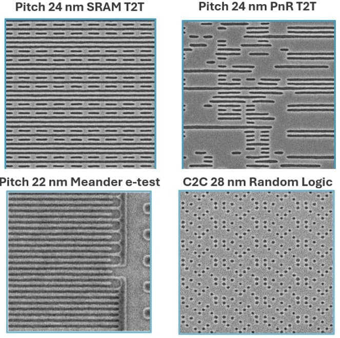
The results were presented at the 2026 SPIE Photomask Technology + EUV Lithography Conference. Imec patterned line-and-space structures down to 22nm pitch, alongside 24nm SRAM layouts, 24nm place-and-route structures, meander test patterns, and random-logic vias.
Earlier work by imec and its materials partners had demonstrated CAR-based High-NA EUV single patterning at 28nm pitch. The latest development tightens the line pitch by a further 6nm while applying the process to structures that more closely resemble the geometry required in advanced logic interconnect layers.
Chemically amplified resists are already deeply established in semiconductor manufacturing, so extending their useful range could allow chipmakers to retain a mature materials platform on selected High-NA layers rather than changing the scanner, resist chemistry, etch process, and integration scheme simultaneously. That does not make CAR suitable for every future layer, but it gives process teams another option as 0.55-NA exposure enters more aggressive design rules.
The work is based on co-optimisation of the resist, lithography, and downstream etch process. A successful exposure is only the first part of pattern transfer: the resist has to resolve the aerial image with acceptable fidelity before the resulting geometry can be transferred into a functional layer without excessive roughness, collapse, or dimensional loss.
Imec reports good pattern fidelity on meander and forked electrical-test structures down to 22nm pitch. The wider test set included 24nm SRAM layouts with 26nm tip-to-tip spacing, place-and-route patterns with 28nm tip-to-tip spacing, and 28nm centre-to-centre random-logic vias.
The organisation identifies metal-2, via, and metal-to-diffusion layers among the possible applications for CAR-based High-NA single patterning at A14 and A10. Advanced logic flows will still combine several patterning strategies because layer geometry, defect tolerance, process maturity, and cost differ throughout a device.
High-NA EUV raises numerical aperture from 0.33 to 0.55, increasing available resolution but also placing tighter requirements on resists, masks, etch, metrology, and process control. The scanner therefore cannot be qualified independently from the surrounding patterning system, particularly when line dimensions and spaces approach the limits of existing materials.
That integration work is also part of imec’s European NanoIC pilot line, which is targeting semiconductor technologies beyond 2nm. High-NA development inside such pilot-line environments allows equipment, materials, and process suppliers to test combinations before production fabs commit them to high-volume manufacturing.
The latest CAR results provide evidence that a mature resist family still has useful scaling headroom under 0.55-NA exposure. Yield improvement and more aggressive pitches remain development targets, but the demonstrated structures move the technology closer to the logic patterns that process engineers will eventually have to manufacture repeatedly rather than print once for a resolution record.