
IN Brief:
- SY757xx devices distribute low-voltage LVCMOS clocks and translate higher-voltage clock sources for newer SoCs, FPGAs, and CPUs.
- The family operates from 0Hz to 250MHz, with additive jitter specified as low as 26fs.
- Three devices are in volume production, while eight additional family members are sampling.
Microchip Technology has introduced the SY757xx family of 1.2V-output LVCMOS clock buffers, addressing the growing mismatch between established board-level clock sources and processors using lower-voltage timing interfaces. The devices combine clock distribution with voltage translation, allowing higher-voltage sources to drive newer FPGAs, SoCs, CPUs, and AI accelerators without relying on discrete divider networks.
That mismatch is becoming more common as advanced processor and programmable-logic devices move onto lower-voltage I/O while surrounding board components remain on 1.8V, 2.5V, or 3.3V rails. Translating a slow control signal between those domains is relatively forgiving; doing the same with a clock requires closer control of edge shape, duty cycle, phase noise, loading, and added jitter.
Microchip specifies an operating-frequency range from 0Hz to 250MHz across the new portfolio, with additive jitter as low as 26 femtoseconds for the family. The devices support a variety of input arrangements and supply levels, including configurations capable of translating clock signals from 3.3V circuitry down to the 1.2V level required by newer processor platforms.
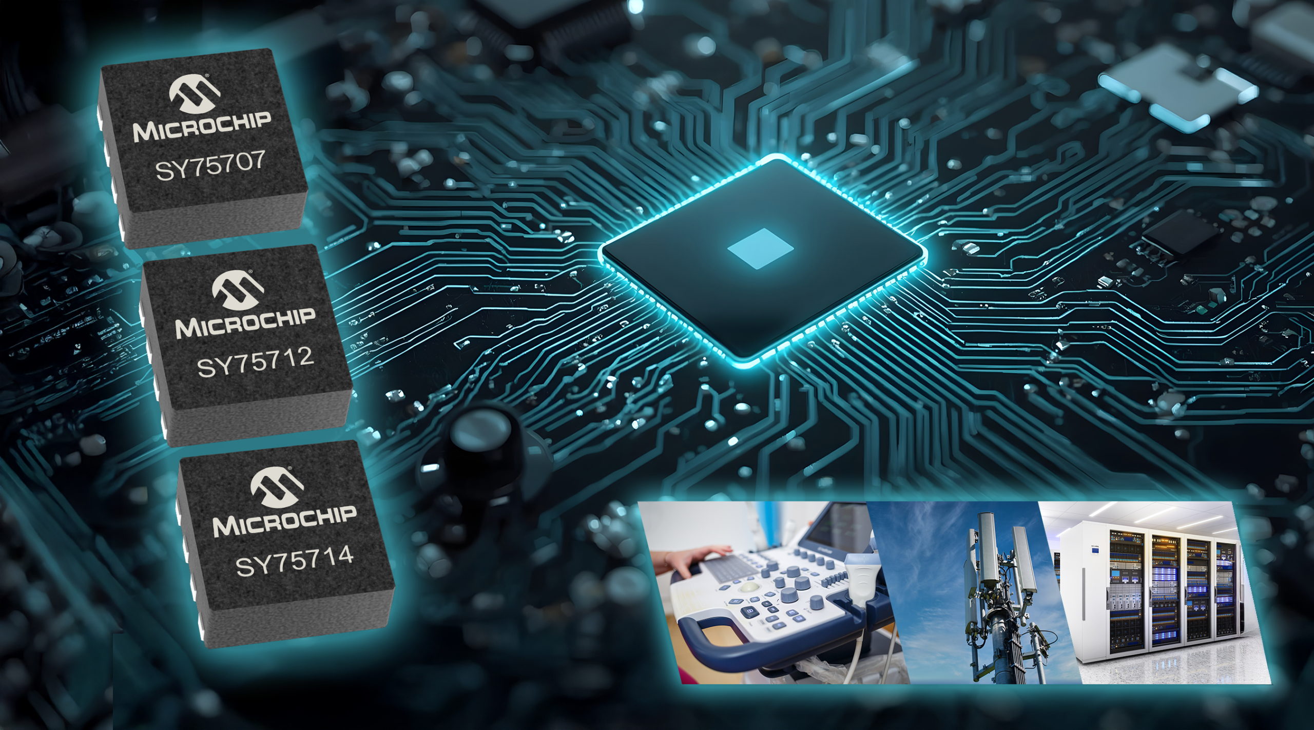
The company has launched three devices directly into volume production. SY75707TWL-TR accepts a differential input and provides two LVCMOS outputs in an eight-pin VDFN package. SY75712TWL-TR and SY75714TWL-TR provide two and four LVCMOS outputs respectively and operate across 1.2V to 1.8V output rails in eight-pin TDFN packages.
Another eight SY757xx family members are sampling in limited volumes. Those devices extend the combination of input and output arrangements, with options covering single-ended 1.2V to 3.3V LVCMOS inputs, lower-voltage single-ended sources, differential 1.8V to 3.3V inputs, and output-enable fanout configurations.
The translation function removes one source of uncertainty from the clock tree. A resistor divider can reduce a signal’s amplitude but does not provide the same controlled switching behaviour as a characterised clock buffer across process, voltage, temperature, load, and edge-rate variation. Additional loading or poorly controlled thresholds can distort duty cycle and reduce timing margin even where the resulting waveform still appears electrically valid.
A dedicated buffer also isolates the original clock source from multiple receiving devices. Fanout becomes important when one oscillator or timing generator has to feed several FPGAs, processors, or peripherals, because adding loads directly changes the electrical conditions seen at the source. The buffer presents a defined input while driving the downstream branches separately.
Microchip is targeting embedded vision, video processing, AI and machine-learning acceleration, industrial control, IoT, networking, communications, and signal-processing hardware. Those applications increasingly combine large processors and FPGAs with older peripheral or timing devices, making mixed-voltage clock distribution a board-level integration problem rather than an unusual corner case.
The 26fs figure should be read as the best specified additive-jitter performance across the family rather than assuming every device produces that result under every condition. Timing performance depends on device configuration, input source, measurement bandwidth, frequency, supply noise, and board implementation, so detailed selection still requires the individual datasheet rather than the family headline.
The same caution applies to signal integrity more broadly. A clock buffer does not remove the need for controlled return paths, sensible placement, decoupling, impedance management, and attention to crosstalk. What it does provide is a device designed and characterised specifically for moving a timing signal between voltage domains rather than asking a passive network to perform that job indirectly.
The production status makes the launch immediately relevant to current designs. SY75707, SY75712, and SY75714 can already be ordered in volume, while the additional sampling parts broaden the architecture available for forthcoming boards as 1.2V timing interfaces become more common across high-performance digital devices.

