IN Brief:
- Qualcomm has validated first-generation HBC silicon using memory read/write tests and computational workloads with randomised weights and activations.
- The architecture places processing closer to memory, with wafer bonding and fault-management techniques supporting its physical integration.
- A data centre product has completed tapeout, while early testing of a logic base bonded to DRAM tiers is progressing.
Qualcomm Technologies has completed physical-silicon validation of its first-generation HBC near-memory computing architecture, testing memory read/write operations and computational pathways using randomised weights and activations at production-representative dimensions. The results advance a hardware development programme intended to reduce data movement during AI inference, alongside work to integrate processing circuitry with bonded DRAM.
Memory access is a major constraint in large AI computing systems because processors repeatedly need information stored outside their immediate execution resources. Model parameters and intermediate values must be supplied to the computing units at rates sufficient to maintain the intended workload throughput. When the available memory bandwidth cannot keep pace with computation, processor resources may spend part of their time waiting for data.
Moving that information also consumes energy. Electrical signals travel through on-chip interconnects, package structures, and interfaces between processing and memory devices, each contributing to the cost of transferring data. The number of transfers and the distance over which information moves consequently influence the energy required to execute an AI workload, particularly when the same model data is accessed repeatedly.
Qualcomm’s HBC architecture places computation closer to memory, with the aim of reducing the amount of information that must travel through conventional processor-to-memory paths. This changes the physical relationship between storage and the operations performed on its contents. The eventual benefit depends on how effectively an application can use the near-memory processing resources and how much data still needs to move to other parts of the system.
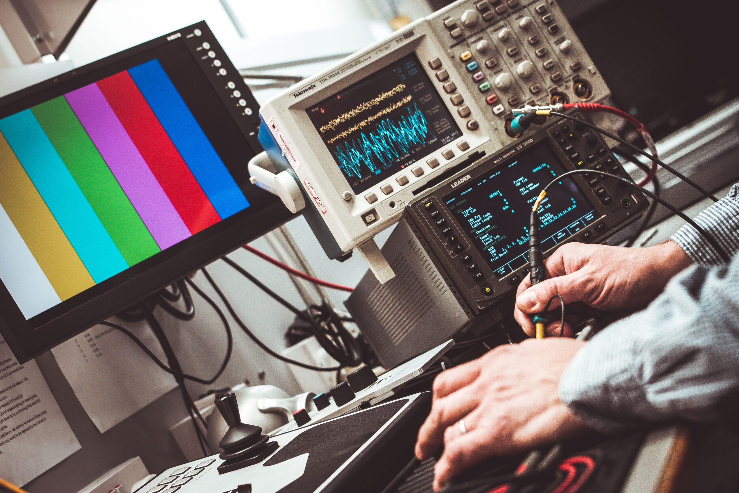
The company’s latest validation used industry-standard automated test equipment to exercise actual semiconductor devices. Engineers tested the complete memory read/write path and computational operations involving randomised model weights and activations. Running these operations in physical silicon provides evidence about the implemented data pathways beyond what can be established through architectural simulation or isolated circuit models.
Production-representative dimensions are important because data organisation and access patterns influence how memory and processing circuits interact. A calculation that operates correctly on a small test structure may encounter additional constraints when the amount of data or the number of operations increases. Qualcomm’s tests therefore examined the data paths at dimensions selected to reflect the intended hardware architecture, although the company has not supplied a complete independent benchmark dataset for a commercial accelerator.
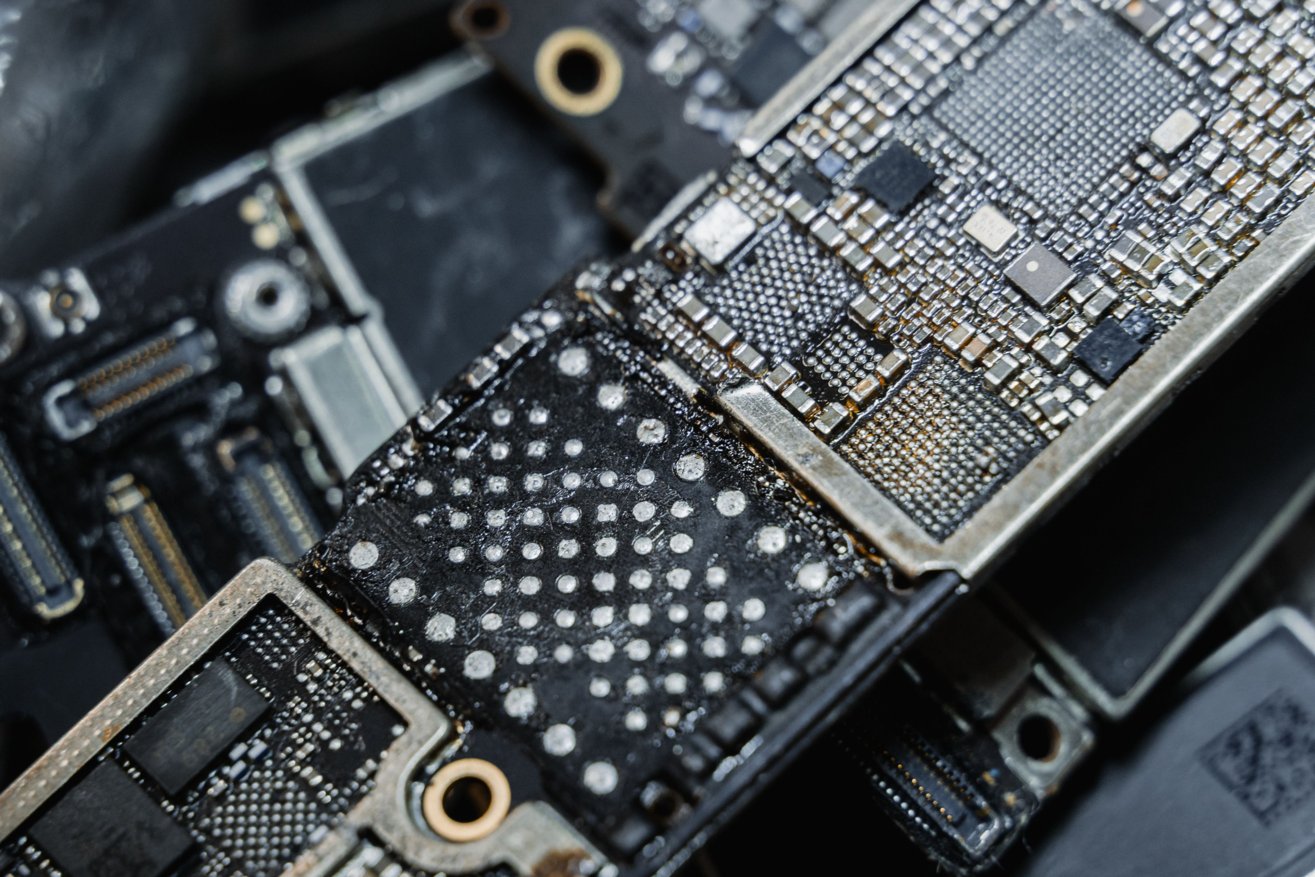
The silicon work follows several development stages covering architecture design, semiconductor processes, test vehicles, and integration methods. Qualcomm has collaborated with foundry and assembly partners on wafer-to-wafer bonding across multiple technology generations. Bonding provides a method of joining semiconductor layers with dense electrical connections, allowing memory and associated logic to be integrated more closely than separate conventional packages.
Those connections must maintain suitable electrical characteristics across the bonded interface. Alignment, process variations, defects, and the condition of the joined surfaces can affect whether individual connections function correctly. The resulting assembly must also manage heat generated by the processing circuitry and memory, making mechanical and thermal validation part of the manufacturing development process.
Qualcomm reports that electrical, thermal, and physical foundations have been evaluated through dedicated test vehicles and working silicon. These activities establish information about the manufacturing structures and device behaviour before the complete commercial product has finished development. Successful test-vehicle measurements provide evidence for the selected processes, while later system integration must demonstrate that the combined architecture performs as intended.
The company has also incorporated redundancy, remapping, and test methods to address defects within memory structures. Redundancy allows suitable spare resources to replace defective ones, while remapping changes the assignment of logical memory locations so that identified faults can be avoided. The effectiveness of those techniques depends on the physical memory organisation, available spare capacity, and the nature of defects encountered during manufacturing.
Such fault-management methods become important when several semiconductor layers are integrated into one assembly. Defects affecting a memory tier or an electrical connection may influence the usability of a larger structure, making manufacturing yield dependent on both the individual components and the interfaces joining them. Testing must therefore identify relevant failure modes while providing information needed to determine whether an assembly satisfies its acceptance criteria.
Qualcomm states that its measured silicon results support bandwidth and energy-efficiency improvements. Its published comparisons are based on first-generation HBC silicon measurements normalised to target operating conditions and compared with published specifications for competing products. Final performance remains dependent on implementation, workload, and system configuration, so those estimates should not be treated as independently measured throughput or power consumption for a completed data centre product.
The development programme has nevertheless progressed beyond isolated research structures. Qualcomm reports that a data centre product has completed tapeout, moving the design into the manufacturing stage. Early bring-up work involving a logic base with bonded DRAM tiers is also yielding results, providing an additional integration step towards the intended product architecture.
Bring-up involves establishing that fabricated hardware can be powered, controlled, and exercised through its required interfaces. Subsequent work must verify sustained operation, thermal behaviour, memory reliability, and computational performance under workloads appropriate to the finished system. Those tests will establish how successfully the first-generation silicon and bonding processes translate into usable computing hardware.
Near-memory processing also requires decisions about which computations should execute close to stored data. Workloads involving substantial movement of model parameters may benefit from a different distribution of processing resources than tasks dominated by operations performed elsewhere. The architecture’s system-level efficiency will therefore depend on software execution, data placement, and the balance between local computation and communications with other processing devices.
Qualcomm has now validated the principal first-generation memory and computation pathways in physical silicon while continuing product integration with bonded DRAM. The next development milestones are the bring-up and qualification of complete devices, followed by measurements establishing the sustained performance and power characteristics of the resulting data centre hardware.