IN Brief:
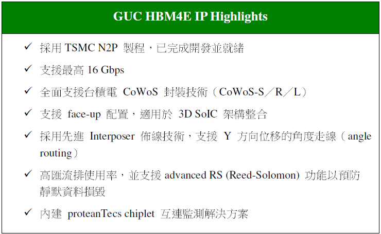
- GUC's HBM4E PHY and controller reaches 16Gbps and uses TSMC's N2P process for advanced AI ASIC programmes.
- The design has been adopted by customers and taped out with CoWoS-L, following GUC's silicon-proven 12Gbps HBM4 generation.
- A face-up SoIC-X implementation adds dedicated TSVs for signals and feedthrough power delivery into vertically stacked silicon.
Global Unichip Corporation has completed the design of a 16Gbps HBM4E PHY and controller for TSMC’s N2P process, with the interface IP already adopted in customer AI ASIC programmes and taped out using CoWoS-L packaging.
The development follows GUC’s 12Gbps HBM4 implementation on TSMC N3P, which the company describes as silicon-proven. The new HBM4E generation raises the per-pin transfer rate to 16Gbps while moving the interface onto a newer logic process and packaging stack.
GUC is careful to distinguish the maturity of the two generations. Its 12Gbps HBM4 IP has completed silicon validation, whereas the 16Gbps HBM4E design has completed design work, attracted customer adoption, and reached tape-out. Working-silicon validation therefore remains a later milestone for the new interface.
HBM performance depends on more than memory-device speed. The PHY has to preserve signal integrity across an extremely wide interface, while the package must deliver current to the memory and compute die without noise or voltage drop consuming the reduced margins created by faster signalling.
GUC says it uses proprietary interposer routing techniques to optimise both signal integrity and power integrity and supports several CoWoS packaging configurations. The announced tape-out uses CoWoS-L, which combines local silicon interconnect structures with redistribution technology to connect large compute devices and high-bandwidth memory inside an advanced package.
The company is also preparing a face-up HBM4E version for TSMC’s SoIC-X technology. This implementation includes dedicated through-silicon vias for signal input and output as well as feedthrough power delivery to an upper die, creating a route for HBM interfaces within vertically integrated chip architectures.
Three-dimensional integration turns power delivery into part of the interface design. A die placed above another device cannot rely solely on conventional package connections beneath it, so power and signals have to pass through the silicon stack while resistance, switching noise, thermal concentration, and routing density remain within acceptable limits.
GUC is positioning the HBM4E interface alongside its GLink and UCIe die-to-die technologies. The combined portfolio addresses horizontally connected chiplets, vertically stacked silicon, and high-bandwidth memory, reflecting the way advanced AI ASICs increasingly depend on several interconnect layers rather than one monolithic die.
The HBM4E PHY also incorporates proteanTecs interconnect monitoring. GUC says the technology improves visibility during PHY test and characterisation and can continue monitoring performance and reliability once the device is operating in the field.
Embedded telemetry becomes more useful as interface margins narrow because failures may arise from interaction between the logic die, package, interposer, power network, and memory stack. Additional observability can help distinguish those effects during characterisation and later operation rather than reducing every fault to a pass or fail at the external interface.
The 16Gbps development raises the bandwidth available from a given memory interface without relying solely on additional HBM stacks. That is attractive in AI accelerators where memory bandwidth increasingly limits how effectively large compute arrays can be kept supplied with data, but higher signalling rates also make package loss, power delivery, and timing closure more demanding.
GUC’s position as an ASIC design and production services company places the HBM interface inside a wider packaging and system-integration programme. Customers still have to choose memory configuration, thermal architecture, package topology, and power delivery, but aligning the PHY with N2P, CoWoS-L, and SoIC-X reduces the number of interfaces being developed independently.
The next milestone is silicon. Tape-out confirms that the HBM4E design has reached manufacturing, but returned devices will still have to demonstrate 16Gbps operation across the voltage, temperature, and process conditions required by customer ASICs. That validation will determine whether the higher-speed interface can deliver the margin expected from the completed design.