IN Brief:
- The VIS and NXP joint venture completed the Tampines fab after 22 months of construction and has entered risk production.
- Volume manufacturing is scheduled for the first quarter of 2027 across 130nm to 40nm specialty processes.
- Capacity is expected to reach about 44,000 300mm wafers per month by 2029, with around 1,600 jobs planned.
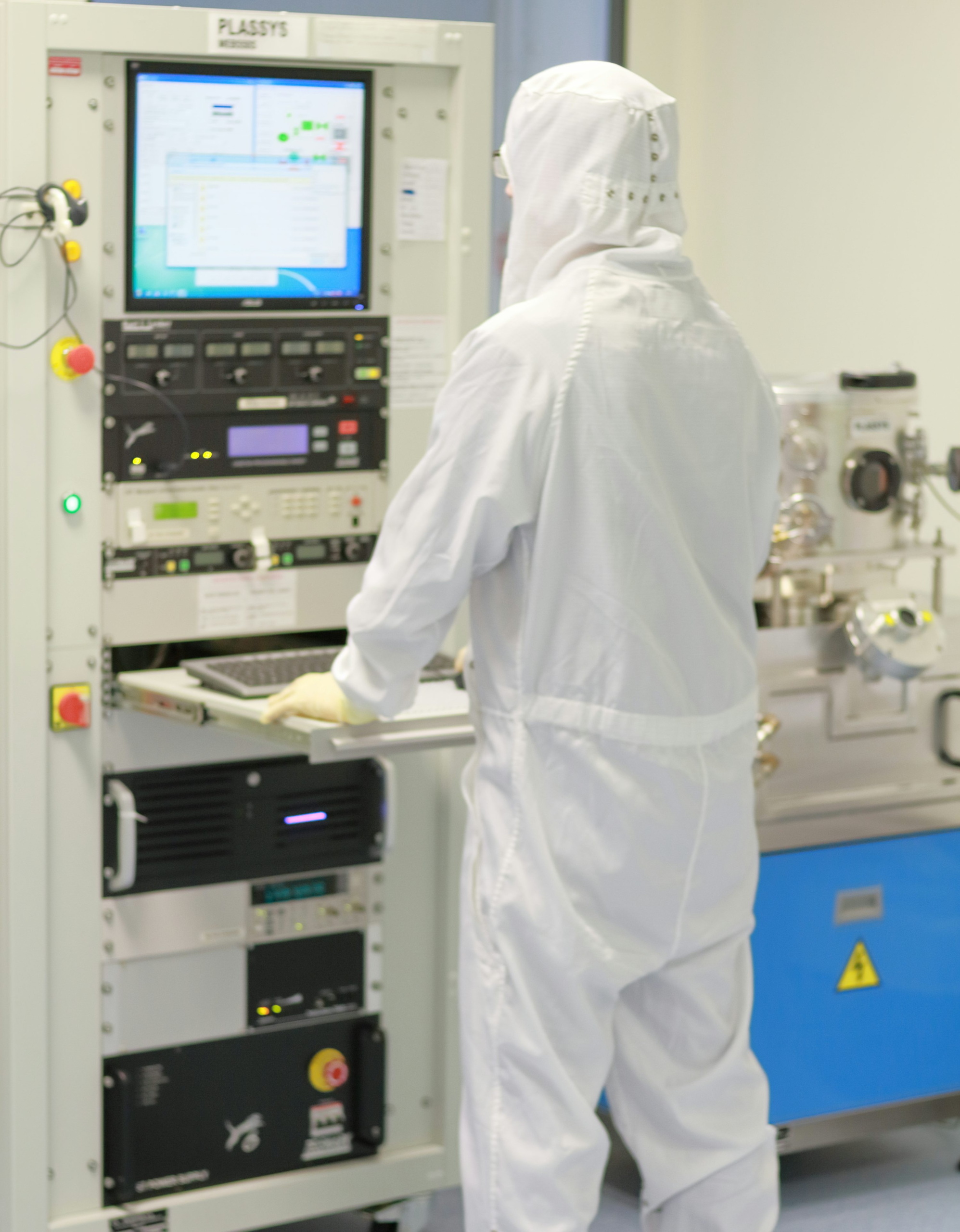
VisionPower Semiconductor Manufacturing Company has opened its first 300mm semiconductor fab in Singapore and entered risk production, moving the Vanguard International Semiconductor and NXP joint venture from construction towards commercial manufacturing.
The Tampines facility was completed after 22 months of construction and has processed its first sample lot, with VSMC reporting yield above 99%. Volume production is scheduled to begin during the first quarter of 2027.
The fab will support process technologies from 130nm to 40nm for mixed signal, power management, analogue and interposer applications. Target markets include high performance computing, mobile, automotive and industrial electronics alongside consumer products.
Those process nodes sit well behind leading edge logic in terms of geometry, but they remain fundamental to electronic systems. Power management, analogue interfaces, mixed signal functions and many automotive devices depend more heavily on voltage handling, embedded functions, process stability and qualification than on maximum transistor density.
Moving those products onto 300mm wafers can improve manufacturing economics by placing more die on each wafer. The advantage is only realised when yield and tool utilisation remain high enough to offset the cost and complexity of operating the larger wafer format.
That makes the reported first sample yield noteworthy, although it is not a substitute for volume production data. A sample lot exercises only part of the manufacturing challenge. The factory will still have to maintain yield as product mix expands, more tools enter sustained operation and customer qualifications impose different process requirements.
VSMC expects monthly capacity to reach approximately 44,000 300mm wafers by 2029. The site is also expected to create around 1,600 jobs, making it a sizeable addition to Singapore’s established semiconductor manufacturing base.
The company has designed the fab around a highly automated production model using digital management and artificial intelligence systems. Automation is already deeply embedded in semiconductor manufacturing, where wafers move through hundreds of tightly controlled process steps and small excursions can affect material that has accumulated considerable value.
New factories nevertheless have to build operating experience. Process recipes, equipment matching, maintenance cycles and statistical controls all have to perform consistently across shifts and over long production runs. Yield learning therefore continues well after the first functional wafers have moved through the line.
The VSMC structure also gives NXP a strategic manufacturing relationship without requiring it to own the entire facility. NXP has described the joint venture as part of a hybrid manufacturing strategy combining internal and external capacity, while VIS contributes its foundry operating experience.
That arrangement is particularly relevant for automotive and industrial semiconductors, where customers often expect supply commitments over longer product lifetimes than in consumer electronics. Manufacturing capacity has to remain available well after the initial device launch, while process changes and second sourcing can require lengthy qualification programmes.
The facility is separate from Singapore’s broader semiconductor research and industry initiatives announced during the same period. Those programmes address ecosystem development and future technology capability, whereas VSMC has reached a physical manufacturing milestone: construction is complete, tools are processing wafers and the factory is preparing for customer volume production.
Its process range also gives the site a broader role than one product family. Mixed signal and power management technologies can serve multiple end markets, allowing the foundry to distribute utilisation across customers and applications rather than depending entirely on one semiconductor cycle.
The commercial test will arrive as risk production turns into qualification and volume manufacturing. Semiconductor fabs generate their economics through sustained yield, throughput and utilisation, not simply installed cleanroom capacity.
VSMC has now crossed the point at which the Singapore site stops being principally a construction project. The next milestone is the first quarter of 2027 volume start, followed by the longer ramp towards the 44,000 wafer monthly capacity planned for 2029.