IN Brief:
- AlixLabs has begun a six-month Atomic Pitch Splitting evaluation within the imec-coordinated NanoIC pilot line.
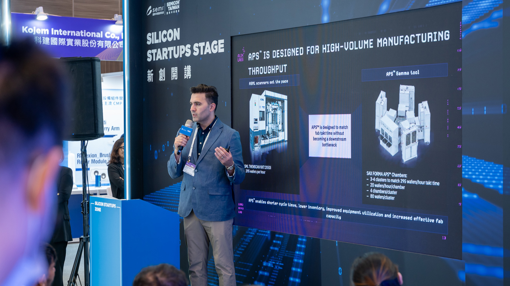
- APS selectively divides pre-patterned features using atomic layer etching, doubling line density with fewer process stages than conventional multi-patterning routes.
- The programme will generate full-wafer and integration data intended to support later equipment qualification and high-volume manufacturing decisions.
AlixLabs has begun a six-month evaluation of its Atomic Pitch Splitting technology within the NanoIC pilot line coordinated by imec, moving the Swedish company’s atomic-layer-etch process into an advanced semiconductor manufacturing environment.
The project combines AlixLabs’ APS process with imec lithography, process integration, and metrology infrastructure. Work will focus on full-wafer performance, integration behaviour, and the process data needed to assess whether APS can progress towards equipment qualification and high-volume manufacturing.
APS starts with structures that have already been patterned and selectively divides them using atomic layer etching. One original feature can be split into two lines, doubling pattern density without introducing another conventional lithography exposure for the pitch-splitting step.
Atomic layer etching removes material through controlled surface reactions, allowing the amount removed during each process cycle to be tightly limited. AlixLabs is applying that control to pattern multiplication, using the existing geometry as part of the process rather than repeating the full sequence of coat, expose, develop, deposit, and etch stages associated with some multi-patterning schemes.
Conventional advanced patterning can use approaches including litho-etch-litho-etch, self-aligned double patterning, and self-aligned quadruple patterning when one exposure cannot provide the required feature density. These methods extend established lithography but also add processing, overlay requirements, metrology, chamber utilisation, and defect opportunities.
Reducing the number of patterning stages could alter those costs, provided the resulting structures meet dimensional and yield requirements. APS therefore has to demonstrate more than a narrow line pitch. Across-wafer uniformity, selectivity, line-edge behaviour, defectivity, process repeatability, and compatibility with surrounding deposition and lithography steps determine whether an etch concept can enter a manufacturing flow.
The NanoIC programme moves that assessment outside AlixLabs’ own development environment. NanoIC is a European pilot line aimed at advanced system-on-chip technology and gives participants access to semiconductor process infrastructure intended to bridge research and later industrial deployment.
The company says potential customers requested validation in an advanced pilot environment as part of their assessment of APS. The six-month project is intended to provide the integration evidence and full-wafer data needed before semiconductor manufacturers consider later qualification stages.
The work follows the June launch of Sax Forma, AlixLabs’ first commercially available APS equipment platform. That earlier development moved the process into customer evaluation hardware; the NanoIC project now tests the underlying technology inside a separate advanced manufacturing environment.
AlixLabs has also continued work on the hardware needed to industrialise the process. A Sax Forma beta chamber entered final assembly with VDL ETG Projects in August, with installation in the company’s Lund laboratories planned before the end of the year.
The distinction between process validation and equipment validation remains important. A patterning method may perform correctly on experimental wafers while the production tool still has to meet requirements around chamber matching, uptime, contamination control, maintenance intervals, wafer handling, throughput, and statistical process control.
NanoIC provides a route to examine the process side using lithography, metrology, and integration infrastructure representative of advanced semiconductor development. Successful results would then support later work around Sax Forma qualification and direct evaluation by prospective manufacturing customers.
APS is not being presented as a replacement for advanced lithography. The method depends on a pre-patterned structure and is intended to operate alongside lithography by modifying selected features after the initial pattern has been created. Its commercial case rests on reducing the burden of additional patterning stages at layers where etch-based pitch splitting provides sufficient control.
That position becomes more relevant as leading-edge manufacturing combines EUV, DUV, deposition, etch, metrology, and computational process control rather than relying on one exposure technology for every critical layer. Each additional stage has to justify its contribution against cost, cycle time, yield, and cleanroom capacity.
The six-month NanoIC programme should provide a more representative dataset for that comparison. AlixLabs now has a commercial equipment platform and an external pilot-line evaluation under way; the remaining threshold is whether APS can maintain its claimed simplification benefits under full-wafer conditions while meeting the process-control standards expected in volume semiconductor manufacturing.