IN Brief:
- The agreement transfers imec GaN-on-silicon process, device and epitaxy technology to Polar Semiconductor.
- The initial proposed enhancement-mode GaN portfolio spans 40V to 650V on 200mm wafers.
- IC-Link will provide access to design and manufacturing services, with production qualification milestones still undisclosed.
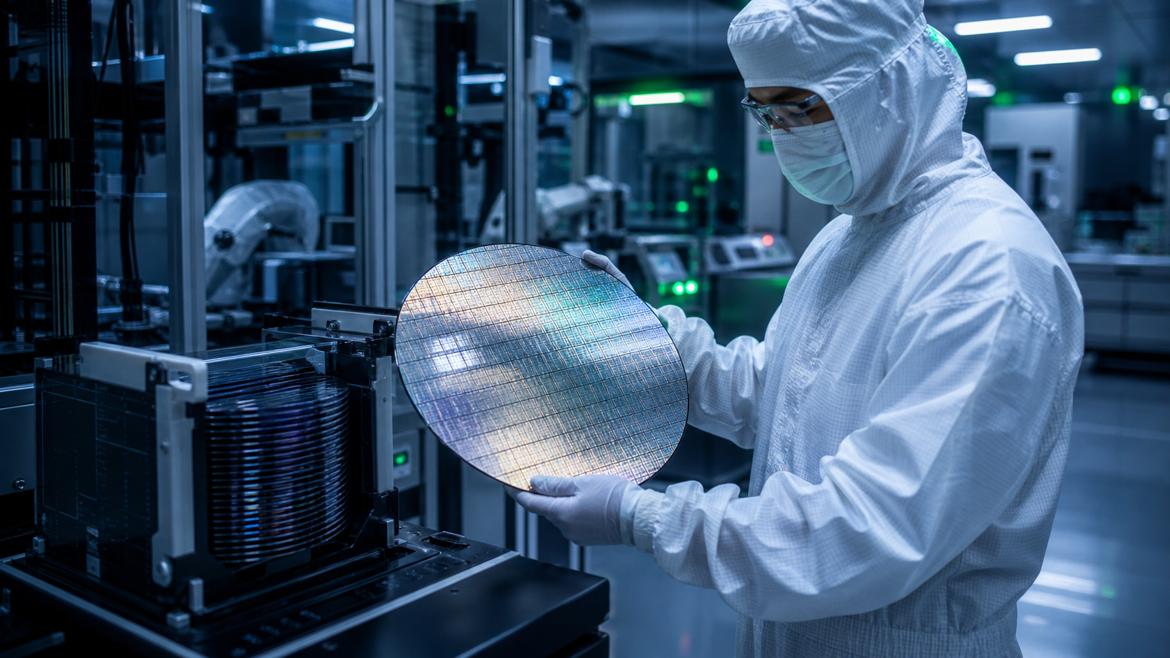
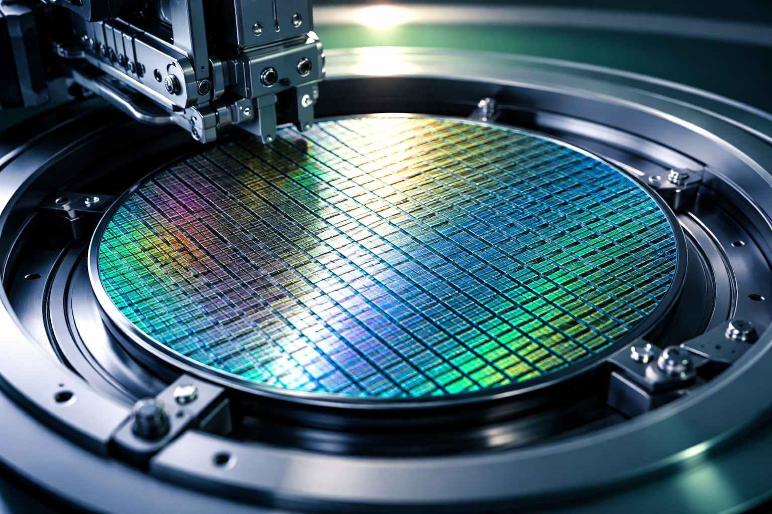
Polar Semiconductor has agreed to introduce a gallium nitride manufacturing process developed by Belgian research organisation imec at its foundry in Bloomington, Minnesota. The collaboration, involving imec’s IC-Link design and manufacturing service, is intended to provide 200mm wafer production of enhancement-mode GaN power devices for customers developing electronic power converters.
The agreement transfers imec’s GaN-on-silicon process, device and epitaxy technology to Polar, with an initial voltage range from 40V to 650V. The partners identify applications in data centres, vehicles, industrial power systems, aerospace and defence. Their longer-term plans include extension outside the first voltage range, although the announcement does not specify production volumes, qualification dates or when particular devices will become commercially available.
Enhancement-mode GaN transistors are normally off when no suitable gate-drive signal is applied. That behaviour is significant in many converter designs because power switches are expected to remain non-conducting during start-up and some fault conditions. GaN devices can offer fast switching and low associated charge compared with alternative technologies, but the useful performance depends on the device structure, operating voltage, thermal design and the gate-drive and protection circuit chosen around it.
Manufacturing the devices on silicon substrates gives the process a route into established semiconductor fabrication equipment. The 200mm wafer format, often described as eight inches, is compatible with an extensive installed industrial fabrication base, although adapting a foundry line still requires equipment, process control and materials integration suited to GaN epitaxy. Transferring a research process into repeatable commercial manufacture involves validating more than the transistor’s headline electrical parameters.
Control over crystal defects, wafer uniformity, device leakage and breakdown characteristics affects how reliably a power device can be produced across the wafer. Engineers must also characterise dynamic on-resistance, switching behaviour, temperature sensitivity and long-term stability, as laboratory performance does not by itself establish acceptable manufacturing yield. Wafer-level and package-level qualification remain necessary steps before a customer can specify the technology for demanding automotive or industrial duty cycles.
Polar already specialises in power, high-voltage and sensor semiconductor processes, including bipolar-CMOS-DMOS technologies and established transistor families. Its manufacturing site therefore provides a different industrial environment from a research pilot line, with the equipment, process monitoring and customer supply obligations of a merchant foundry. The collaboration is intended to combine that manufacturing base with imec’s device development work rather than create an entirely new fabrication plant.
IC-Link will support customers seeking early access to the GaN technology and provide design-to-manufacturing services as the process moves towards production. The availability of a coordinated route from initial device design through process transfer may reduce the number of separate organisations a customer must manage. However, access to a process does not automatically provide a qualified finished component, a packaging solution or a completed converter reference design; these remain separate engineering and supply decisions.
The 40V-to-650V span addresses a broad but not uniform set of electrical systems. Lower-voltage converters might prioritise high switching frequency and compact components, while higher-voltage applications require stronger isolation and careful management of switching stress. The partners also point towards emerging 800V-to-12V data centre distribution arrangements, where designers must decide how to partition voltage conversion, protection and current delivery through the rack.
GaN’s fast electrical transitions can improve conversion efficiency, but they can also increase susceptibility to layout parasitics, ringing and electromagnetic interference. In industrial systems the device is only one part of the engineering problem: board layout, magnetic components, thermal management and fault handling establish whether a theoretical switching advantage survives in the finished supply. The licensing agreement supplies a potential manufacturing foundation for those designs, rather than a guaranteed system-level efficiency result.
Polar and IC-Link must now transfer and qualify the process within a production foundry environment. The companies have not published design rules, device qualification results or a timetable for customer production orders, so the full 40V-to-650V range cannot yet be described as available in volume.