IN Brief:
- A first approximately $10bn fab at Malta, New York, is expected to begin operation in 2029.
- A second approximately $10bn facility remains contingent; each fab is projected to support 900,000 300mm wafers annually at full capacity.
- A separate $955m adjustment to the existing CHIPS award concerns photonics, SiGe and advanced packaging investments.
GlobalFoundries has been selected as the technology provider and operator for two proposed semiconductor fabrication plants at Malta in New York State. The US–Japan initiative provides for an initial investment of approximately $10bn in the first 300mm fab, with a further investment of approximately $10bn envisaged for a second facility. The announcement does not mean either factory is operating, and the additional facility remains conditional on further investment decisions.
GlobalFoundries expects to break ground on the first plant later in 2026 and has identified 2029 as its planned operational date. The company describes the existing Malta site as permitted and prepared for expansion, allowing some infrastructure to be shared with established manufacturing operations. Construction, production-equipment installation, process qualification and customer validation must still take place before commercial wafers can be supplied.
The company projects annual capacity of around 900,000 300mm wafers for each fully operational factory. If both projects proceed and achieve that level, combined capacity would be approximately 1.8 million wafers a year. These are future capacity estimates, not figures for current production. The actual number of usable chips derived from those wafers will depend on chip area, process complexity and yield.
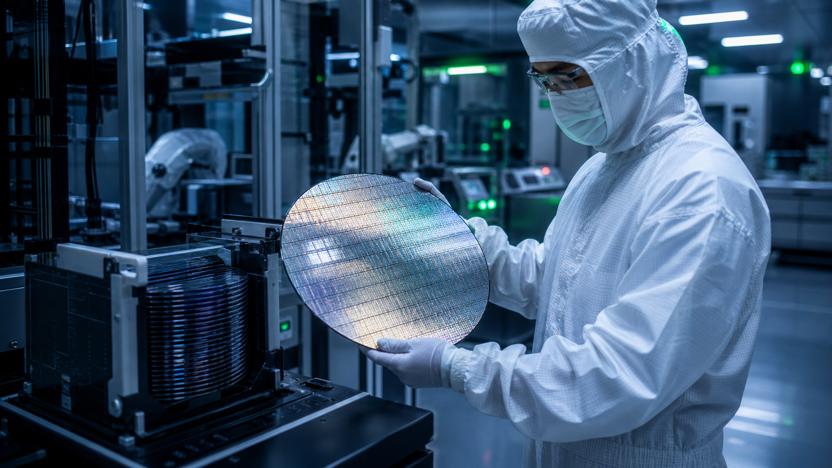
A semiconductor fab requires multiple stages of deposition, lithography, etching, cleaning, implantation and metrology, with many operations repeated as layers are formed. Each stage must remain within a defined process window if complete devices are to function consistently. Increasing wafer throughput therefore involves not simply adding floor area, but also providing reliable utility systems, skilled manufacturing staff and equipment that can achieve repeatable results.
The US–Japan agreement envisages up to $21bn of funding, with Japan providing investment and GlobalFoundries contributing its technology and operational capabilities. The proposed first and second factories have separate financial milestones. Reporting the combined figure without that qualification would imply a greater degree of project certainty than the announcement supports.
The investment is intended to increase US semiconductor capacity for automotive, industrial and connected infrastructure markets. These applications rely on a variety of differentiated processes, including analogue, mixed-signal, RF and embedded-device technologies. GlobalFoundries has an established portfolio spanning these areas, but the company has not assigned a definitive process technology or customer production mix to every planned line in the two factories.
Industrial equipment manufacturers frequently need long product support lives and components that remain qualified through successive equipment generations. Manufacturing continuity and reliable process control are therefore important considerations alongside the number of wafers produced. Building a new fab does not eliminate component supply constraints immediately because products require transfer, validation and stable yields before volume output can be relied upon.
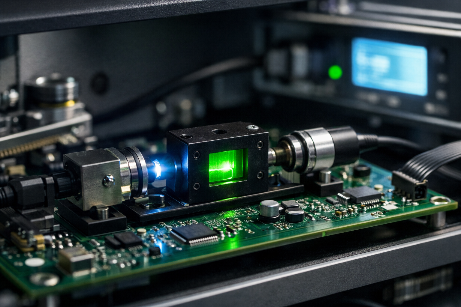
The company has also agreed to amend its existing US CHIPS and Science Act award, reallocating $955m towards investments in silicon photonics, silicon-germanium and advanced packaging at Malta and Burlington, Vermont. That change is a separate adjustment to an existing support arrangement, not a further addition to the two-fab construction budget. The technologies involved are relevant to optical interconnects, high-frequency devices and advanced semiconductor packaging.
A separate arrangement would provide the US Department of Commerce with an equity interest in GlobalFoundries of approximately 4%. The agreement’s financial arrangements must be distinguished from its industrial milestones, especially while construction and technology qualification remain incomplete. The company has identified customers and suppliers associated with its wider manufacturing plans, but has not disclosed binding production volumes for every participant.
GlobalFoundries forecasts more than 1,000 high-skilled manufacturing jobs and about 27,000 construction and ecosystem roles associated with the proposed programme. These employment figures are projections tied to future investment. The announced development is the selection of the operator and establishment of a financing framework; evidence of production will depend on subsequent construction, tool installation and qualification milestones.