IN Brief:
- ENDOPACK embeds SiC MOSFET dies into the traction inverter PCB structure.
- Shortened current paths are intended to reduce stray inductance and packaging complexity.
- Automotive adoption depends on thermal cycling, serviceability and manufacturing qualification.
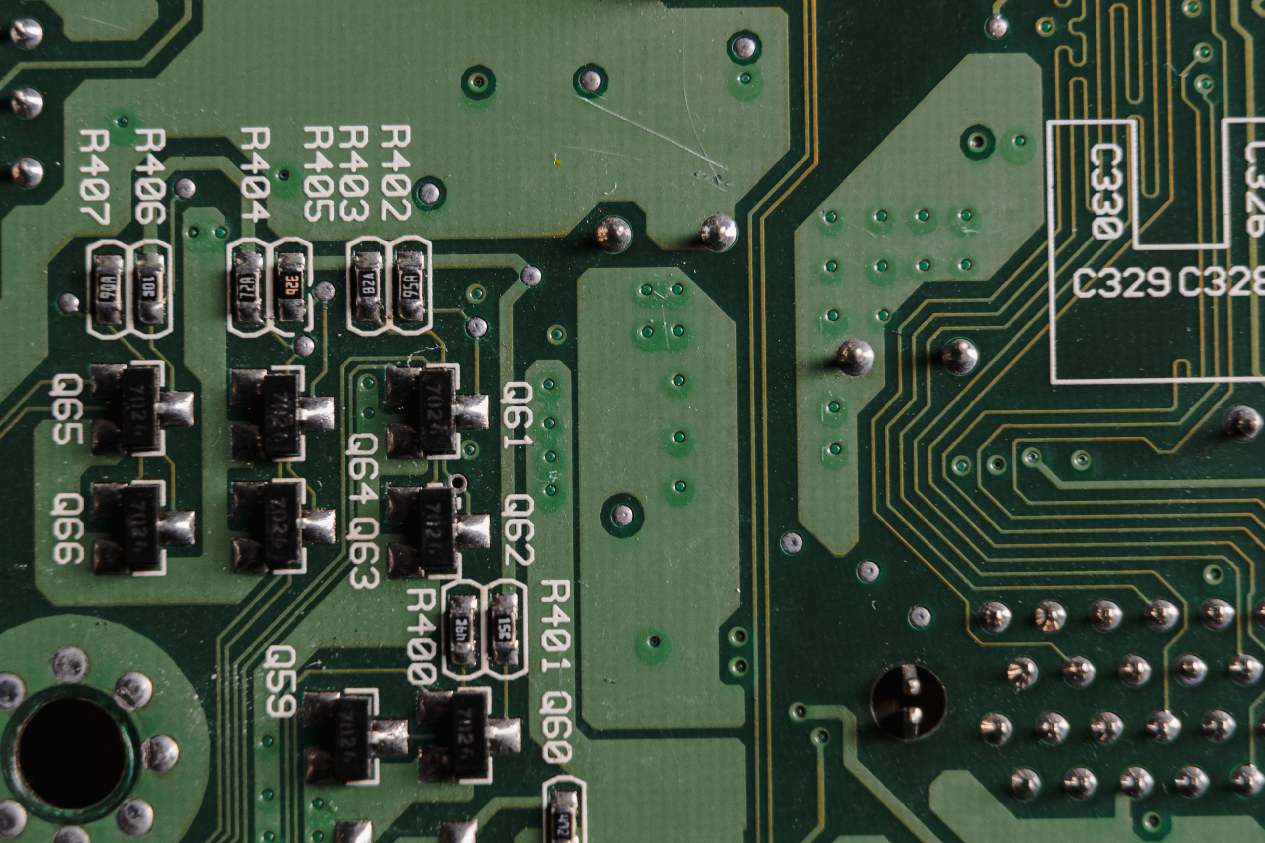
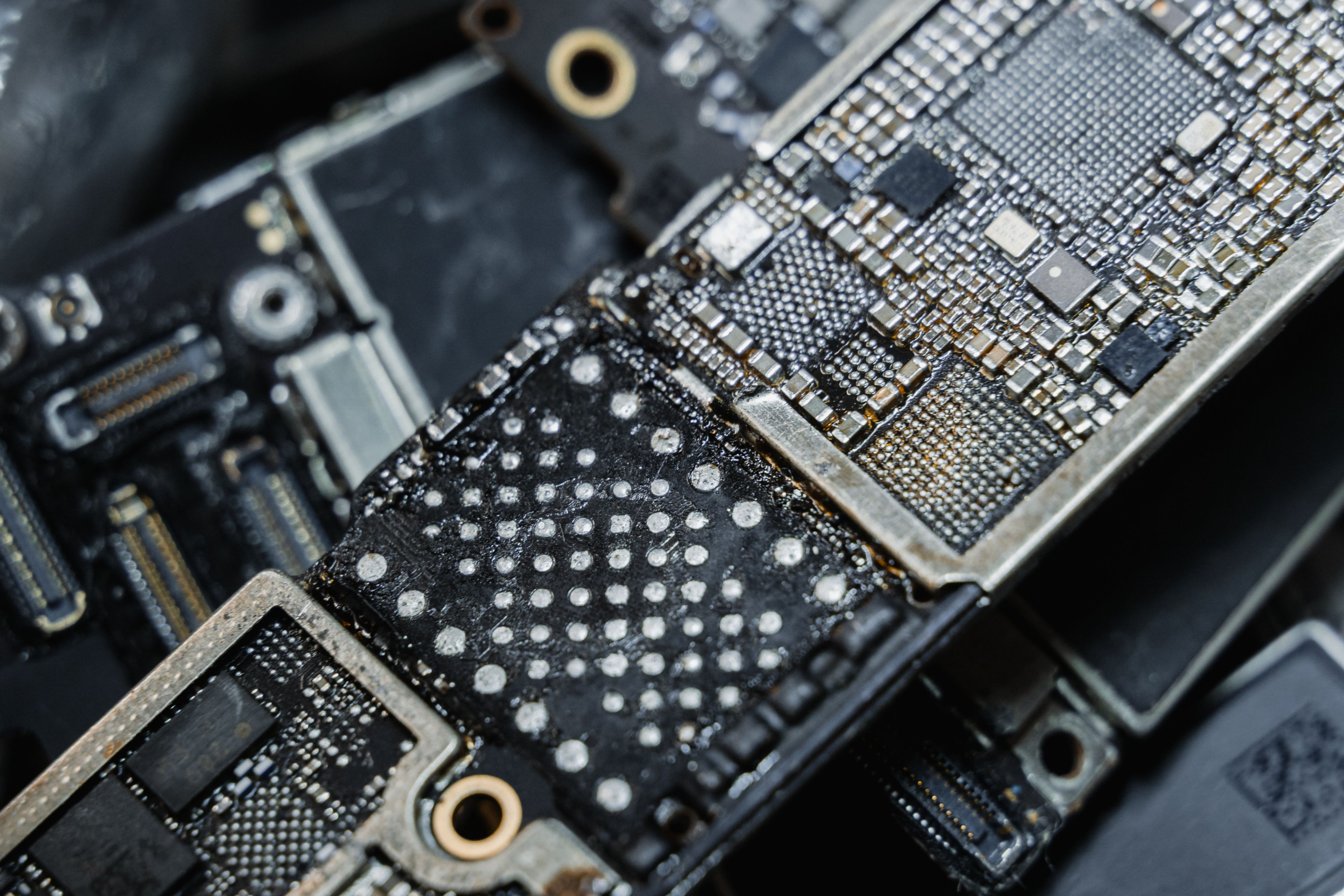
Infineon has introduced ENDOPACK Cell, a high-voltage chip-embedding approach for automotive traction inverters that places 1200V CoolSiC MOSFET technology within the printed circuit board structure of a traction inverter. Rather than building the power stage around a separate conventional semiconductor module mounted above a substrate, the design integrates the device into the board architecture. The company says the approach is ready for mass production, with vehicles using ENDOPACK Cell planned for series production in 2027. That is a forward vehicle programme, not evidence that all automakers have already completed design qualification.
The interconnect architecture is central to the engineering proposal. A traction inverter repeatedly switches substantial current through semiconductor devices to control an electric motor. Even a relatively short conductor introduces stray inductance, which can create voltage overshoot and ringing during fast switching.
Infineon reports inductance below 2nH for its embedded arrangement against a stated 20nH conventional reference. The comparison concerns specified structures and should not be read as a universal figure for every inverter module or installation.
Lower inductance can permit designers to exploit rapid silicon carbide switching more effectively while moderating electrical stress. Infineon also reports 30% lower switching losses and approximately 99.5% efficiency under its stated CLTC conditions. These are company-reported results dependent on the test configuration, rather than independently established improvements across all complete electric vehicles. Losses from copper, magnetics, cooling equipment, control electronics and the motor still affect overall propulsion efficiency and usable driving range.
Embedding power dies changes packaging freedom. The number and location of semiconductor cells can be adapted within a board instead of being constrained by a fixed module outline. Infineon describes the potential to reuse common designs across several vehicle platforms and cites development cycles up to three times faster than traditional approaches.
These advantages depend on the manufacturer retaining suitable board and thermal designs when changing current rating, power density or physical installation constraints. Reuse still requires checking each variant against its electrical operating envelope.
Heat extraction is a decisive issue. Semiconductor junctions generate losses inside a structure with multiple dielectric and conductive layers, so the thermal path to a heatsink must be characterised alongside the current path. Thermal cycling can strain interfaces between materials with different expansion characteristics.
Insulation coordination also needs to account for the 1200V devices, voltage transients and manufacturing tolerances. A successful board design has to remain robust after years of vibration, repeated acceleration and charging-related temperature changes.
Production moves some of the qualification burden into PCB fabrication and assembly. Layer registration, embedded-component placement, lamination, void control and nondestructive inspection are critical when the die cannot be accessed like a conventional board-mounted package. A defective embedded power cell may affect the serviceability of an assembly and require different failure-analysis methods. Board suppliers and automakers will need repeatable processes, defined test coverage and clear acceptance criteria before broad deployment.
Inverters also place substantial demands on the control electronics around their switching devices. Gate-drive timing, fault monitoring and current measurement must remain robust when the physical arrangement of power semiconductors changes. An embedded board might improve the main current path while creating new challenges for accessing test points or repairing an assembly.
Designers should compare the proposed architecture with established modules under identical electrical loads, cooling conditions and driving cycles, using measured loss breakdowns rather than a single headline efficiency percentage. Qualification will require both production-process evidence and application-level tests.
Infineon’s prototype and simulation work identifies a peak power-density potential of 200kW per litre and a potential vehicle-range improvement of 7%. Both are conditional engineering claims, particularly the vehicle-level projection, which depends on drivetrain architecture and duty cycle. The immediate significance is the option to configure a SiC inverter power stage through an embedded PCB manufacturing route. The planned 2027 vehicle introduction will provide a more tangible test of that route’s manufacturability and long-term performance.