IN Brief:
- OnRamp offers selected developers foundry-engineering consultations and fabrication roadmaps.
- Early access to SP90 development wafers depends on technical fit and capacity.
- The programme targets photonics, sensing, communications and quantum startups.
SkyWater Technology has opened an OnRamp programme intended to give quantum and photonics hardware developers earlier contact with semiconductor foundry engineers. The initiative offers selected teams technical discussions and manufacturing roadmaps, with a potential route towards development wafers in the company’s SP90 silicon-photonics platform. It addresses a familiar obstacle for small hardware businesses: a promising photonic layout cannot be evaluated as a product until a compatible process, design rules, packaging strategy and wafer-manufacturing route have been established. Access to advice should not be confused with a guarantee of free or immediate fabricated samples.
Photonic integrated circuits route and manipulate light through patterned structures rather than relying solely on conventional electronic interconnects. Applications include sensing, communications and quantum systems, where optical phase, propagation loss and the quality of interfaces to detectors or emitters affect usable performance. Small changes in fabrication geometry can influence circuit behaviour. Designers therefore need accurate process-design information, not merely access to generic electronic-layout software, before committing to a wafer run.
The OnRamp model aims to make some of these manufacturing constraints visible earlier. Foundry engineering consultations can help identify whether a proposed structure fits the available material stack, lithographic capabilities and process tolerances. Development teams may then revise their designs before spending money on photomasks or wafer processing. For resource-constrained startups, avoiding an unsuitable tape-out can be more valuable than accelerating a design that cannot be manufactured with an available qualified process.
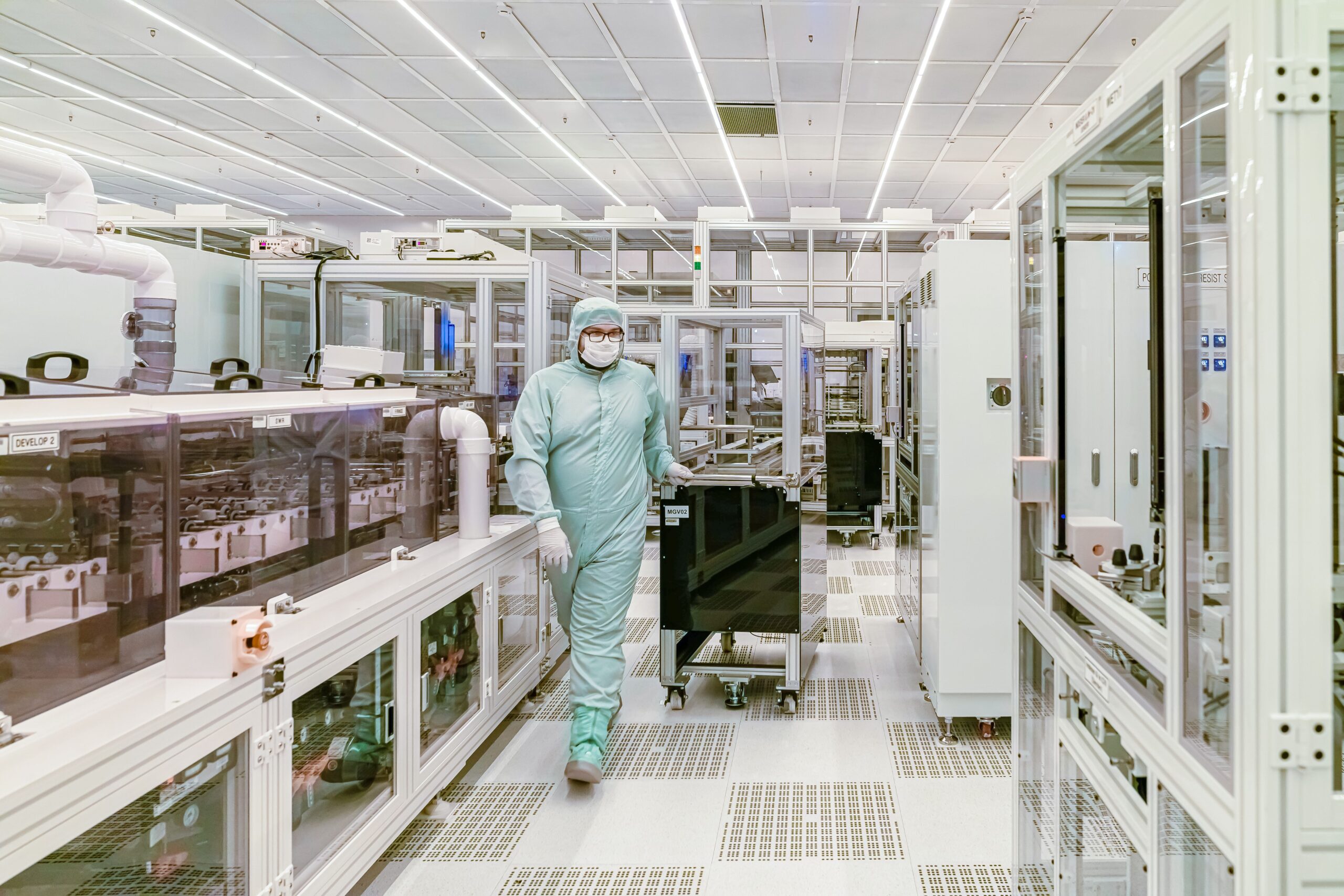
SkyWater’s SP90 programme is associated with silicon nitride photonics and a 200mm wafer manufacturing route. Silicon nitride can be useful where low optical propagation losses and particular wavelength requirements are important, although each process imposes design limitations. Matching a circuit to a foundry platform also involves bends, waveguide spacing, coupling features, testing structures and practical methods for packaging the die. Optical I/O and alignment tolerances can dominate assembly cost even where the wafer-stage circuit performs well.
Early wafer access is conditional on technical suitability and capacity. A company’s willingness to discuss a design is different from accepting it into a scheduled fabrication run, and prototype manufacturing may involve paid slots and contractual conditions. Engineers should establish what data will be returned, whether process variations are characterised and how intellectual property will be handled. Repeatability between a first research batch and later production wafers is especially important when customers require demonstrable yield or long-term stability.
The commercial setting extends beyond photonic components themselves. Quantum hardware firms may need integrated optical routing alongside detectors, lasers, cryogenic electronics or precision timing systems, all of which can create integration challenges outside the foundry’s immediate process. Communications and sensing developers face different certification, optical power and environmental requirements. Foundry guidance cannot replace system engineering, but it can narrow the risk that an otherwise attractive device is incompatible with available packaging and test infrastructure.
Foundry transfer can become especially complex when a prototype relies on laboratory processes that are unavailable in volume fabrication. Different deposition conditions or etch steps may change waveguide roughness, optical loss and device uniformity. A practical manufacturing roadmap should identify which structures can be produced within the standard process and which would require custom steps, additional mask layers or external assembly.
That division affects both prototype budgets and the eventual unit economics. It also helps engineering teams avoid designing around attractive experimental results that are difficult to reproduce in a commercial line.
OnRamp represents an attempt to bring manufacturing realities into early photonic product development rather than waiting until a startup seeks a full production agreement. The decisive indicators will be the number of designs reaching completed runs, their measured yields and whether successful prototypes can progress to repeatable supply. For companies evaluating SP90, the relevant next steps are process-fit assessment, realistic fabrication budgets and a clear plan for turning wafer-level measurements into packaged devices.