IN Brief:
- Villach project targets high-volume GaN power chip manufacture on 300mm wafers.
- Infineon plans about €1.1bn investment by 2034 and €319m in Chips Act support.
- First production is planned for late 2027; ramp-up follows market demand.
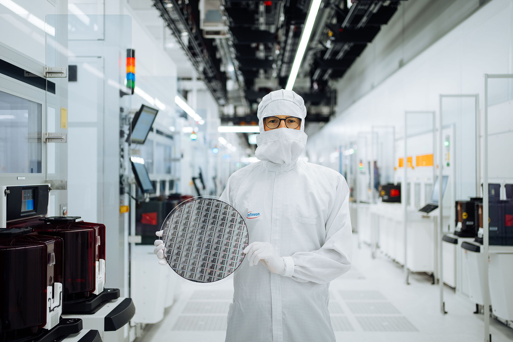
Infineon is preparing a €1.1bn expansion of gallium nitride power semiconductor manufacturing at its Villach site in Austria, with 300mm wafer production due to begin in late 2027. The investment is planned through 2034 rather than being spent at the outset. The company has identified €319m in support under the European Chips Act framework, a contribution that should be distinguished from the total planned expenditure. The project addresses a manufacturing constraint increasingly relevant to designers selecting GaN devices for power conversion: obtaining sufficient capacity, consistent process quality and predictable supply as demand expands.
The choice of 300mm wafers matters because usable surface area rises with the square of wafer diameter. Compared with a 200mm wafer, the larger format offers roughly 2.25 times the gross area, before accounting for edge losses, yields and differences in device layout. More potential die per process cycle can improve economics once equipment utilisation and defect control are established.
Those conditions are important qualifications. Wafer area alone does not translate directly into a corresponding fall in the cost of a tested, packaged power component.
Gallium nitride’s principal engineering appeal is its ability to switch efficiently at comparatively high frequencies in suitable converter topologies. Smaller magnetic components may then become possible, although actual losses depend on gate-drive design, thermal management, parasitic inductance and electromagnetic compatibility. In servers, vehicle chargers, renewable-energy converters and industrial power supplies, power-system architects have to optimise the semiconductor alongside passive components and the wider mechanical package. A chip made on a larger wafer does not, in itself, change these circuit-level trade-offs.
Scaling production also involves moving established processes into a much larger manufacturing flow. Uniformity of deposited layers, wafer bow, lithographic control, metallisation and wafer handling all influence how many functional devices survive fabrication. Process engineers must reconcile high-volume throughput with the leakage, breakdown-voltage and switching characteristics required by customers. Subsequent testing, packaging and reliability qualification can become additional bottlenecks, especially where parts must withstand prolonged exposure to heat, electrical stress and repetitive switching.
Villach already manufactures power semiconductors, so the project will upgrade and use existing cleanroom infrastructure rather than construct an entirely separate operating site. Infineon schedules the start of 300mm GaN production for late 2027, followed by a ramp aligned with customer demand. That interval must accommodate equipment installation, process transfer, validation and customer qualification.
Procurement teams assessing longer-term supply therefore need to distinguish the scheduled first wafers from qualified, high-volume deliveries. The European Commission has approved €319m in state aid, with the formal Austrian funding commitment still subject to the applicable criteria and process.
The European policy context is unusually direct. Support through the Chips Act is intended to reinforce strategic semiconductor supply, but a funding commitment cannot substitute for equipment, skilled staff and qualified production. European equipment and manufacturing specialists could benefit from the build-out while customers assess whether regional capacity reduces the risks associated with long logistics routes. At the same time, competitive pricing and consistent availability will ultimately determine whether device makers place more of their designs on a new manufacturing platform.
Another issue for customers is how devices made on a new wafer diameter will be qualified against existing designs. Electrical parameters may be nominally unchanged, yet a transition in process equipment or manufacturing site can require change notifications and engineering assessment. Buyers of automotive and industrial power components often need evidence of accelerated ageing, electrical robustness and continuity between production batches. Infineon’s capacity investment could strengthen regional availability, but the pace at which different part families migrate to the new process will determine when those benefits become visible to engineers.
For engineers specifying GaN, the near-term task remains to qualify devices against electrical and thermal requirements and identify credible secondary sourcing arrangements. The investment creates a pathway to more 300mm capacity, not proof that existing semiconductor shortages or design-validation obligations have disappeared. The key dates for buyers are the planned start of wafer production in late 2027 and the later stages of the company’s phased €1.1bn programme, when measurable capacity and qualified output should become clearer.