IN Brief:
- Nexperia's GaN expansion covers DC-DC conversion, synchronous rectification, robotics, and high-current power distribution.
- The available GANE0R8-100QTM is rated at 100 V with typical on-resistance of 0.75 mΩ in a 3 × 5 mm PQFN package.
- Six products are available now, with two additional devices, including a 0.32 mΩ variant, scheduled for Q1 2027.
Nexperia has expanded its low- and medium-voltage gallium nitride transistor portfolio with devices designed for high-current power conversion. The eight-product family will cover voltage ratings from 18 V to 200 V, with six devices available initially and two further products scheduled for the first quarter of 2027.
The new devices target DC-DC conversion, synchronous rectification, industrial motor control, robotics, and power distribution in computing infrastructure. Nexperia is combining low on-state resistance with fast switching characteristics and compact packages designed to accommodate concentrated heat generation.
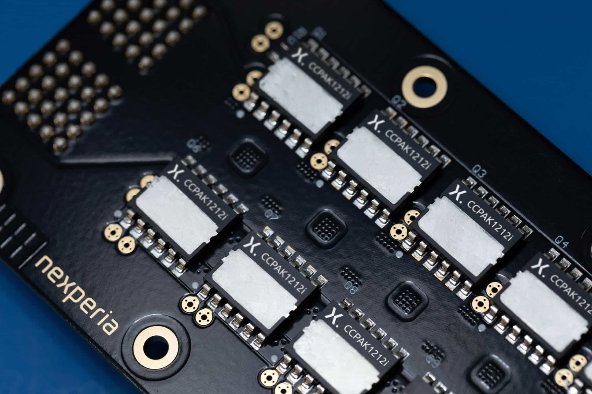
The initially available GANE0R8-100QTM is a 100 V GaN field-effect transistor with a typical on-resistance of 0.75 mΩ. It uses a 3 × 5 mm power quad flat no-lead (PQFN) package, providing a surface-mount format for high-current converter stages.
Five other devices are available across ratings from 25 V to 200 V, with on-resistance values reaching 0.37 mΩ. The forthcoming GANE0R3-015QTL will extend the range to 18 V with typical on-resistance of 0.32 mΩ, but that device is not scheduled for release until Q1 2027.
Low on-resistance is particularly important in converters delivering substantial current. The power dissipated through a conducting transistor increases with the square of its current and its on-state resistance, meaning a relatively small resistance difference can become significant as operating current rises.
At 100 A, for example, a resistance of 0.75 mΩ corresponds to 7.5 W of instantaneous conduction loss. The average loss depends on the current waveform and the time the transistor spends conducting, while resistance changes with operating temperature and the device’s electrical characteristics.
This relationship helps explain the interest in low-resistance switching devices for processor power delivery. A computing system may distribute power at an intermediate voltage before converting it to the much lower voltages used by processor cores, requiring converters capable of delivering high output currents.
Nexperia identifies its lower-voltage devices as options for secondary-side synchronous rectification and conversion from 12 V distribution rails towards sub-1 V processor supplies. Higher-rated devices can be used in primary and secondary conversion stages, including arrangements based on 48 V distribution.
Synchronous rectification replaces a conventional rectifier diode with a controlled transistor in parts of the power-conversion circuit. When correctly driven, a transistor with sufficiently low on-resistance can reduce conduction losses compared with the forward-voltage drop of a diode at the same current.
However, the control circuit must coordinate switching transitions with the behaviour of the rest of the converter. Incorrect timing can introduce additional losses or allow undesirable current paths, particularly in bridge-based configurations with rapidly changing electrical conditions.
GaN transistors support fast switching, allowing converter designers to consider higher operating frequencies. Increasing frequency can reduce the size of some magnetic and passive components, but the available benefit depends on the total losses and the electromagnetic behaviour of the completed circuit.
Transistor selection therefore involves more than comparing RDS(on). Gate charge influences the energy needed to switch a device, while output capacitance affects the energy associated with voltage transitions. These parameters become important where a transistor changes state many times per second.
Nexperia identifies low products of on-resistance and charge-related characteristics among the features of the family. Such figures of merit help compare devices intended for similar operating conditions, although they do not substitute for calculating losses within the intended converter topology.
The new products also support multi-level and stacked conversion architectures. These circuits distribute voltage stress across several switching elements or conversion stages, potentially allowing different device voltage ratings and operating conditions to be used within a wider power-distribution system.
Those arrangements require appropriate control and protection. Voltage sharing, switching timing, and transient behaviour must be managed, since an individual device may experience electrical stress that differs from the nominal division expected during steady-state operation.
Packaging becomes increasingly important as high current is concentrated in compact power stages. Nexperia offers 3 × 5 mm and 3.3 × 3.3 mm PQFN arrangements with exposed pads intended for top-side cooling, providing a path for transferring heat towards an external thermal structure.
The effectiveness of that thermal path depends on the interface material, mounting arrangement, board construction, and available cooling. A device’s small footprint does not independently establish its continuous current capability, particularly where high switching frequency adds further heat to the conduction losses.
Motor-control applications introduce additional operating requirements. Three-phase brushless DC and permanent magnet synchronous motor drives must coordinate switching devices with current measurement, position information, and the selected control algorithm. The chosen GaN devices must withstand the electrical transients and temperature conditions generated by those operating cycles.
Nexperia has made six members of the new family available and plans to complete the eight-device range during Q1 2027. The expansion provides additional low-resistance switching options for conversion stages operating below the company’s newly introduced 750 V silicon carbide portfolio.