IN Brief:
- Sandisk's iNAND CL EM181 is available in 64 GB, 128 GB, and 256 GB configurations using 112-layer 3D TLC NAND.
- The e.MMC 5.1A interface supports HS400 operation, with manufacturer-tested sequential speeds up to 300 MB/s read and 225 MB/s write.
- SmartSLC buffering, configurable SLC storage, error correction, and health monitoring support embedded device storage management.
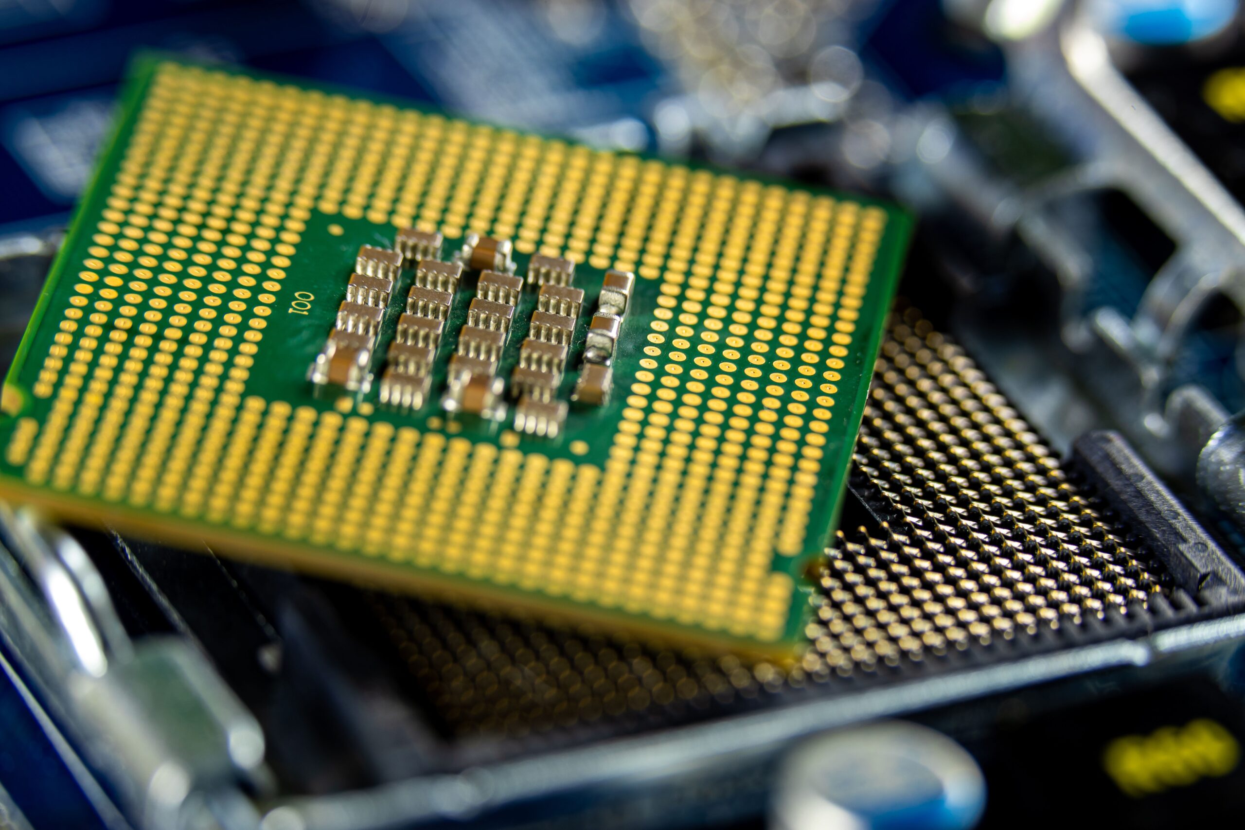
Sandisk has introduced the iNAND CL EM181 embedded flash drive, combining 112-layer three-dimensional NAND memory with an established e.MMC interface for electronic products requiring storage continuity across extended manufacturing lifecycles.
The device is available in capacities of 64 GB, 128 GB, and 256 GB, with all three configurations using the same JEDEC-compatible package. Introduced at electronica 2026 in Munich on 10 November, the product is intended to support migration from earlier embedded flash generations without requiring extensive changes to existing circuit boards.
The CL EM181 uses an e.MMC 5.1A interface with HS400 operation, providing a theoretical bus transfer capability of up to 400 MB/s. Sandisk reports sequential read speeds of up to 300 MB/s and sequential write speeds of up to 225 MB/s under its internal test conditions.
Embedded MultiMediaCard technology integrates NAND flash memory and a storage controller within a single component. The controller manages functions including error correction, logical addressing, wear levelling, and communication with the host processor, reducing the need for the main application to implement these storage management operations directly.
Although newer storage interfaces provide higher transfer rates, e.MMC remains in use across connected products where package compatibility, supply continuity, and established hardware designs are important. Changing to a different interface can require alterations to the processor connection, PCB layout, firmware, and qualification procedures.
Sandisk has retained the established interface while updating the underlying memory technology. The approach allows equipment developers to assess a newer flash generation without automatically changing the entire storage architecture of the host system.
The three capacity options share an 11.5 × 13 × 1.0 mm package with 153 solder-ball connections. A common footprint supports different storage capacities within the same hardware family, although the host software must still be compatible with the selected device configuration and storage capacity.
The memory uses 112-layer three-dimensional triple-level cell NAND technology. Three-dimensional NAND stacks memory structures vertically, increasing storage density without relying exclusively on reductions in the lateral dimensions of individual cells.
Triple-level cell memory stores three bits in each cell by distinguishing between multiple electrical charge states. This provides higher storage density than single-level cell operation, but it introduces different programming and endurance characteristics because the controller must maintain sufficiently accurate distinctions between more closely spaced states.
Sandisk has incorporated SmartSLC technology to support write performance and endurance. The system allocates part of the flash memory to a single-level cell operating mode, providing a buffer in which incoming information can be written before being managed within the wider NAND storage arrangement.
Using an SLC write buffer can improve performance during short bursts of activity, particularly when a host produces data faster than the underlying TLC memory can sustain during direct programming. The benefit depends on the available buffer space, the state of the device, and the controller's background management activities.
The CL EM181 also supports a configurable Enhanced User Data Area, allowing a designated region of storage to operate using SLC characteristics. This provides an option for information that is written frequently or requires a different endurance profile from ordinary data stored in the main user area.
Assigning memory to this mode creates a capacity trade-off. Operating a cell with fewer available charge states can improve its write characteristics, but it reduces the quantity of information that can be stored within the same physical memory area.
The appropriate allocation depends on the application workload. A connected gateway recording frequent system logs may place different demands on storage from a camera writing sequential image data or a monitoring system retaining relatively small configuration files.
Sandisk has not published application-independent endurance ratings or a universal sustained write performance figure for the configurable SLC region. These characteristics must be evaluated according to the capacity allocation, write pattern, and operating conditions of the intended equipment.
The product incorporates low-density parity-check error correction to detect and correct errors in data retrieved from the NAND array. Error correction is particularly important as flash memory cells experience repeated programming and erasure, with their electrical characteristics changing throughout the device's operating life.
Automatic refresh, wear levelling, and block management provide further storage maintenance functions. Wear levelling distributes write activity across available memory regions, while block management handles the allocation and replacement of physical storage areas as the device is used.
Advanced power protection is also included. However, this feature should not be interpreted as a guarantee that every in-progress write will survive an unexpected loss of external power. The complete system still requires suitable shutdown behaviour and data protection arrangements for its application.
A Device Report function provides runtime health and diagnostic information. Such information can assist software in tracking storage condition and identifying developing problems, although the maintenance decisions available to the application depend on the reported parameters and how they are interpreted.
The CL EM181 operates between -25°C and +85°C. This range covers many connected and embedded installations, but it does not establish suitability for equipment requiring the wider -40°C minimum temperature associated with some industrial component specifications.
Data transfer performance also depends on the complete host system. The e.MMC bus limit of 400 MB/s is distinct from the device's measured sequential performance, while small random transfers, sustained writing, and mixed workloads may produce different results.
Sandisk's published performance figures are based on internal testing and may vary with device capacity, host hardware, and usage conditions. They should therefore be treated as product-level reference values rather than guaranteed throughput for every application.
The company identifies connected appliances, gateways, security cameras, and data centre logging systems among its intended applications. Each involves a different combination of capacity, transfer rate, endurance, and service-life requirements, making storage workload analysis necessary before selecting a configuration.
The manufacturer has not disclosed a confirmed volume production timetable for every capacity or a contractual supply period for the new family. The device is listed through Sandisk's commercial product channels, with availability and pricing subject to the applicable purchasing arrangements.
The iNAND CL EM181 provides an updated NAND architecture while retaining e.MMC connectivity. Its value as a replacement component will depend on whether the host system can use the new storage device without substantial changes and whether the selected configuration meets the required write endurance, data integrity, and operating conditions.