IN Brief:
- Vishay and Kaynes Technology signed a binding term sheet on 12 November for a proposed Indian semiconductor back-end manufacturing joint venture.
- Vishay would invest $56.4m for a 49% stake in an existing Kaynes subsidiary, with Kaynes retaining 51%.
- The planned operation would include captive Vishay capacity and possible third-party services; no completed transaction, qualified product line, or start date is confirmed.
Vishay Intertechnology and Kaynes Technology India have signed a binding term sheet for a proposed semiconductor back-end manufacturing venture. Vishay would invest $56.4m for a 49% interest in an existing Kaynes subsidiary, leaving Kaynes with 51%. The planned Indian operation would undertake post-fabrication wafer processing, assembly, test, and packaging for Vishay, with the possibility of serving other chip customers.
Vishay disclosed the agreement in a 12 November filing with the US Securities and Exchange Commission. Definitive contracts, required approvals, and other closing conditions remain outstanding, and the parties have not confirmed completion of an equity transfer. Nor does the term sheet establish that a new jointly owned production line is already qualified or operating.
The Kaynes subsidiary involved is Kaynes Semicon Private Limited. Kaynes has said Vishay is expected to use nearly 90% of the planned manufacturing capacity; this is a projection of prospective demand, not a current utilisation rate. The eventual product mix, production volumes, and space available to third-party customers remain to be defined through the final arrangements.
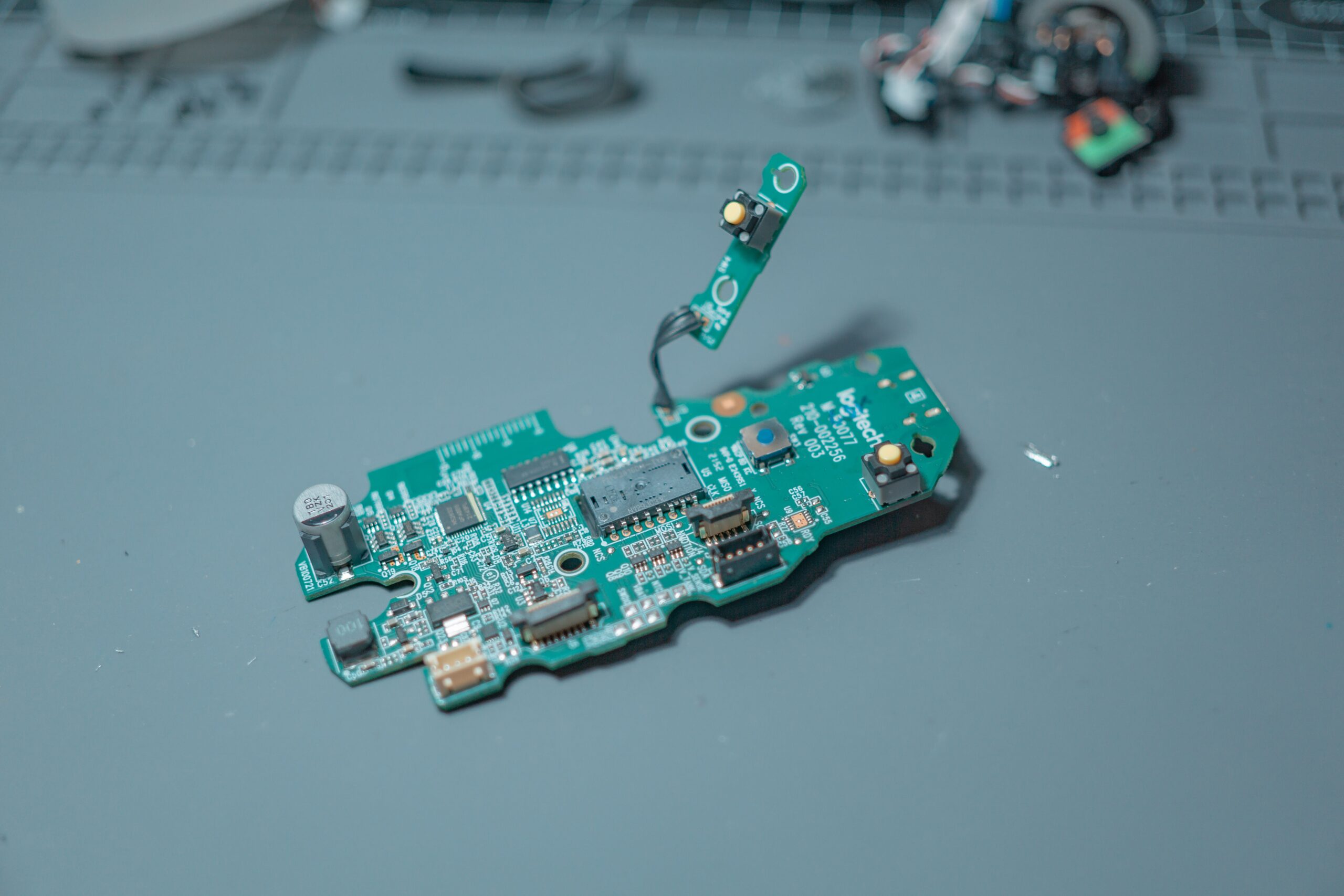
Back-end semiconductor manufacturing starts after the wafer fabrication process. Finished wafer structures may require further preparation before individual dies are attached to a package, provided with electrical interconnections, protected by encapsulation, and inspected and tested. These stages determine how a chip connects to a circuit board and carries current and heat during operation.
Assembly requirements vary considerably between semiconductor products. A power device may need low-resistance connections and an effective thermal path, whereas a precision analogue chip can be sensitive to package stress, parasitic capacitance, leakage, and temperature drift. Choosing the right equipment and acceptance tests therefore depends on the devices Vishay eventually assigns to the venture; the announcement does not name the product families.
Much of the planned work falls within outsourced semiconductor assembly and test, or OSAT, but the venture would also provide captive capacity predominantly intended for Vishay. This may allow equipment and qualification plans to be organised around an anchor customer’s requirements. Work for outside customers would be subject to the parties’ agreed commercial rules rather than an assumption that all capacity is available to the wider market.
The proposed minority investment would still give Vishay specific decision rights over the new business. The SEC filing identifies equipment and vendor selection, internal control and IT systems, auditor appointments, and approval of third-party customers among the areas under Vishay’s control; certain reserved matters would require agreement by both shareholders. These provisions bear directly on process consistency, customer confidentiality, and the specification of manufacturing infrastructure.
Moving an existing chip into a different packaging and test operation requires controlled process transfer. Die attachment, bonding materials, package geometry, thermal interfaces, inspection limits, and electrical test methods have to reproduce the qualified manufacturing result. Even with unchanged silicon, alterations to assembly steps or package materials can affect reliability and trigger further qualification work.
Final electrical testing can measure leakage, switching parameters, voltage thresholds, or analogue accuracy under defined operating conditions. Reliability evaluation may also require environmental and accelerated ageing tests suited to each device family. Neither an agreed product list nor a detailed process qualification programme has been published for the proposed Kaynes venture, so testing capability cannot yet be inferred across Vishay’s entire portfolio.
The partners intend to seek central and state support through India Semiconductor Mission 2.0, according to the filing. Applying for that assistance does not establish that funding has been granted. Any further financing is expected to be contributed broadly in proportion to the respective ownership stakes, but the final project budget and capital spending schedule have not been disclosed.
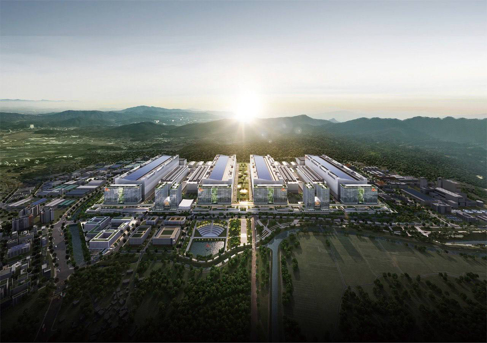
Kaynes is separately developing assembly and test operations in Sanand, Gujarat, including a pilot capability and additional infrastructure. That gives the proposed relationship an existing manufacturing context, but the November filing does not specify which installed tools, buildings, or third-party agreements would be transferred into the venture. The final operational scope will need to be established in the definitive agreements and subsequent capacity disclosures.
Closing the transaction would give Vishay an ownership interest in a proposed Indian back-end manufacturing operation while extending Kaynes’ potential semiconductor workload. Before devices can be supplied from the venture, the partners must settle the contractual structure, identify the product transfers, assign process equipment, and complete the necessary qualification work. The reported November milestone is the binding term sheet; production output, third-party services, and government support are still prospective.