IN Brief:
- Trinity Fab is planned inside SK hynix’s first Yongin memory plant, with shared testing space for domestic equipment and materials suppliers.
- The project is budgeted at approximately KRW874.6bn, with a separate multiyear supplier-support programme valued at KRW1.4tn.
- The facility remains under construction, with equipment installation and full operational access planned during 2027.
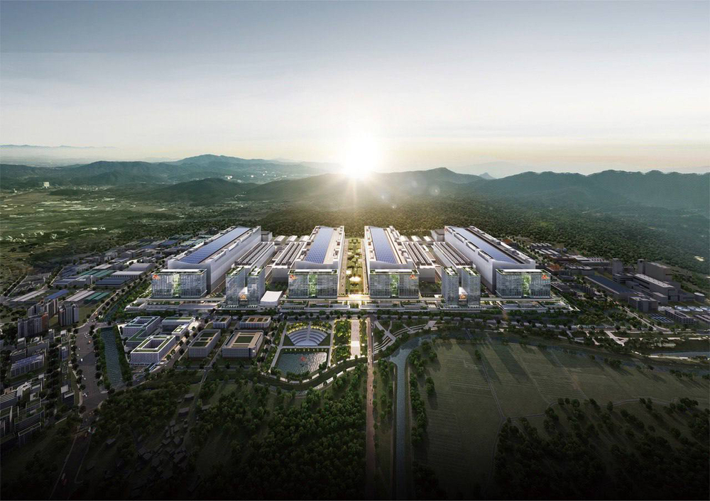
SK hynix has disclosed further construction and operating details for Trinity Fab, a semiconductor supplier test facility inside its first Yongin memory plant in South Korea. The planned testbed will let materials, components, and equipment suppliers assess processes closer to the conditions of a production memory fab. Construction continues, and routine use by suppliers has not begun.
Journalists visiting the site in November described a test area of about 3,300 square metres on the third floor of the Yongin No. 1 fab. Its proximity to the memory clean room is intended to let visiting suppliers work with SK hynix process engineers without relying entirely on distant pilot facilities. Access to a nearby test operation does not mean a supplier has already qualified its product for the memory production line.
The separate Trinity Fab investment is reported at KRW874.6bn, with funding involving SK hynix and public-sector partners. SK hynix has also outlined a five-year KRW1.4tn programme supporting domestic materials, parts, and equipment suppliers through research, testing, production, and sales development. The larger total should not be described as additional construction expenditure for Trinity Fab, nor counted as a newly completed investment.
Trinity Fab was already under construction before the November site visit. Engineers and contractors were completing technical floors and other internal works, with equipment installation and commissioning still ahead. Current reporting targets full operation during the fourth quarter of 2027, rather than presenting the partly completed space as a functioning commercial test line.
A semiconductor process line requires tightly controlled utilities as well as specialist machinery. Lithography, deposition, etching, cleaning, metrology, and inspection depend on stable power, cooling, chemical supply, water quality, gas distribution, and cleanroom conditions. Raised floors and service spaces accommodate airflow and utility routes, which helps explain why the interior construction remains a substantive part of preparing the test environment.
The facility is being prepared for a mixture of process tools and measurement systems used to assess materials and equipment under manufacturing conditions. Korean reports refer to dozens of tools, with some citing around 55 units. Since equipment inventories and configuration details differ across reports, the precise number should remain provisional until the operator confirms the installed and commissioned set.
A supplier may demonstrate acceptable results in a laboratory while still encountering contamination, variation, or throughput problems during a manufacturing transfer. Etch chemistries, deposited films, wafer handling equipment, and inspection techniques interact with the preceding process steps and the factory’s operating conditions. A representative test line can expose those interactions before a material or machine is introduced into volume production.
Direct contact with SK hynix process engineers could make it easier to distinguish a defect in the supplier’s device from a problem in the surrounding process flow. An apparent film defect may originate in an earlier cleaning step, while measured tool performance can depend on incoming wafer characteristics and the chosen recipe. Qualification will need controlled runs and repeatable metrics rather than a single successful demonstration.
The programme is intended to shorten the path from supplier development to industrial use. Some November reports describe a target reduction from roughly three years to two, but that is a prospective objective, not an outcome measured at Trinity Fab. The actual interval will depend on test capacity, recipe maturity, the type of equipment or material, and acceptance requirements imposed by the eventual manufacturing customer.
Shared access may reduce the infrastructure burden on smaller Korean equipment and materials companies that cannot build production-scale test facilities of their own. Each participant will still have to prepare samples, process recipes, engineering staff, and valid performance data, with testing time allocated among potentially competing suppliers. Access rules, confidentiality, and ownership of process information will be important to the facility’s operation, although the detailed arrangements have not been released.
The broader Yongin development is intended to create substantial memory-chip manufacturing capacity. Trinity Fab has a different function: it will test and evaluate suppliers’ manufacturing technologies, rather than produce saleable memory devices as its primary purpose. Passing through its processes could support subsequent supplier qualification, but it will not itself represent a procurement commitment by SK hynix.
The published schedule still depends on completion of cleanroom services, equipment installation, and the qualification of the test environment before participating suppliers can use it routinely. The November reporting provides new physical detail and a clearer operating plan, while any claimed reduction in qualification time will need to be measured after test campaigns and transfers into production have taken place.