IN Brief:
- Samsung Electro-Mechanics and NVIDIA have amended their existing semiconductor substrate supply agreement.
- The expanded relationship includes cooperation involving high-reliability MLCC technology for AI infrastructure.
- Manufacturing activity at Sejong and Busan supports the existing substrate partnership, although new component volumes remain undisclosed.
Samsung Electro-Mechanics and NVIDIA have expanded their semiconductor component cooperation, extending an existing package substrate partnership to include high-reliability multilayer ceramic capacitor technology for accelerated computing platforms.
The companies have also amended their substrate supply agreement to improve manufacturing capabilities at existing production facilities, supporting NVIDIA’s plans to increase production of current and next-generation computing systems.
The agreement builds on the strategic partnership established in October 2026, when Samsung Electro-Mechanics outlined plans to supply advanced semiconductor package substrates for NVIDIA’s computing and networking products.
The latest development broadens that relationship rather than creating a new supplier arrangement. The companies have identified multilayer ceramic capacitors, or MLCCs, as an additional area of cooperation, while maintaining their focus on advanced substrates.
These components perform different functions within a computing system, but both are important to the electrical design and manufacture of high-performance semiconductor hardware.
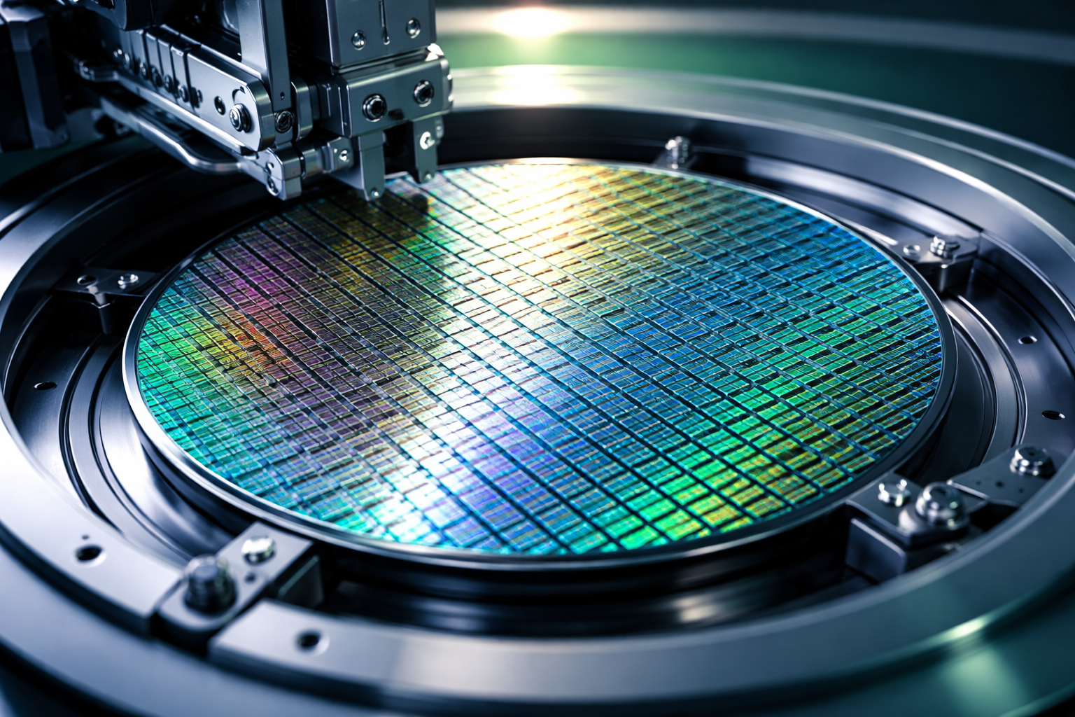
Package substrates provide the interconnection structure between semiconductor devices and the surrounding assembly. They accommodate electrical connections for power delivery, high-speed communication, and other functions within increasingly complex processor packages.
Advanced processors and multi-chip assemblies require substantial numbers of connections, often within a limited physical area. The substrate must route those signals while maintaining suitable electrical characteristics and mechanical stability.
Manufacturing becomes more demanding as connection density increases. Fine conductor patterns, multilayer structures, and precise alignment are needed to support sophisticated semiconductor packages.
Substrate warpage is another consideration. Materials expand and contract during manufacturing and operation, potentially introducing mechanical distortion that affects the reliability of assembled components.
Samsung Electro-Mechanics identifies fine-pattern processing and the ability to control substrate warpage among the capabilities supporting its advanced package substrate business.
The October agreement involved dedicated substrate manufacturing operations in Sejong and Busan, South Korea. The November amendment is intended to improve operational capabilities at existing facilities and support increased production for NVIDIA.
The companies have not disclosed a precise increase in Samsung Electro-Mechanics’ manufacturing capacity under the amendment.
NVIDIA has separately announced quantified expansion targets involving other suppliers, including Kinsus, but those figures should not be applied to Samsung Electro-Mechanics.
The inclusion of MLCC technology adds a different component category to the relationship.
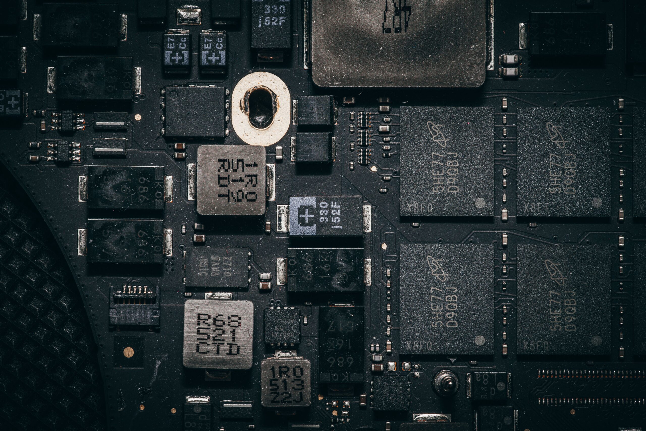
MLCCs are widely used within electronic power distribution networks to provide decoupling, filtering, and local energy storage. They are particularly important where semiconductor devices draw rapidly changing currents from their supply rails.
Advanced computing processors contain circuits that can change operating states quickly, producing variations in electrical demand. Those changes can cause disturbances in the voltage supplied to the device unless the surrounding power network is designed appropriately.
Capacitors positioned at different points in the power distribution system help provide transient current and reduce unwanted voltage variation.
The required arrangement depends on the processor’s supply characteristics, circuit board construction, package design, and the frequency range over which power disturbances must be controlled.
MLCCs can provide useful capacitance within compact components, allowing them to be placed close to power connections on dense electronic assemblies.
Their effectiveness is not determined by nominal capacitance alone. Equivalent series resistance, inductance, frequency response, operating voltage, and temperature characteristics all influence their behaviour.
Some ceramic dielectrics also exhibit changes in effective capacitance when a DC voltage is applied. This can reduce the capacitance available in operating conditions compared with the nominal rating.
The mechanical reliability of MLCCs must also be considered. Stress caused by circuit board bending, thermal expansion, or assembly processes can damage ceramic components if the package and installation are not suitably controlled.
These considerations become more demanding in computing equipment with high component densities and substantial thermal loading.
Samsung Electro-Mechanics already manufactures MLCCs for demanding electronics applications. Its expanded cooperation with NVIDIA links those capabilities more explicitly with the components used around accelerated computing platforms.
However, the companies have not identified the specific capacitor part numbers, volumes, or qualification schedules associated with the new cooperation.
The announcement should therefore not be interpreted as confirmation that particular NVIDIA products have completed qualification of newly specified Samsung Electro-Mechanics capacitors.
NVIDIA is also extending manufacturing arrangements across other parts of its semiconductor supply chain, including package substrates, advanced packaging, and semiconductor assembly.
These activities address different production constraints. Additional substrate capacity can support the construction of more packages, while sufficient availability of supporting passive components remains necessary for the completed electronic systems.
Manufacturing expansion requires more than additional equipment capacity. Semiconductor suppliers must establish stable processes, qualify their products, and meet the electrical and mechanical requirements of their customers.
The revised Samsung Electro-Mechanics agreement provides a further step in that process. Its immediate scope covers the existing substrate manufacturing relationship and expanded MLCC cooperation, while detailed component supply commitments remain undisclosed.
Subsequent production and qualification milestones will determine how the arrangements translate into increased component availability for NVIDIA’s computing platforms.