IN Brief:
- Aeluma has agreed to purchase an AIXTRON G10-AsP MOCVD system for photonic semiconductor manufacturing.
- The customised equipment supports automated processing of 150 mm and 200 mm gallium arsenide and silicon substrates.
- The investment is intended to expand manufacturing capability for high-speed photodetectors and quantum dot lasers.
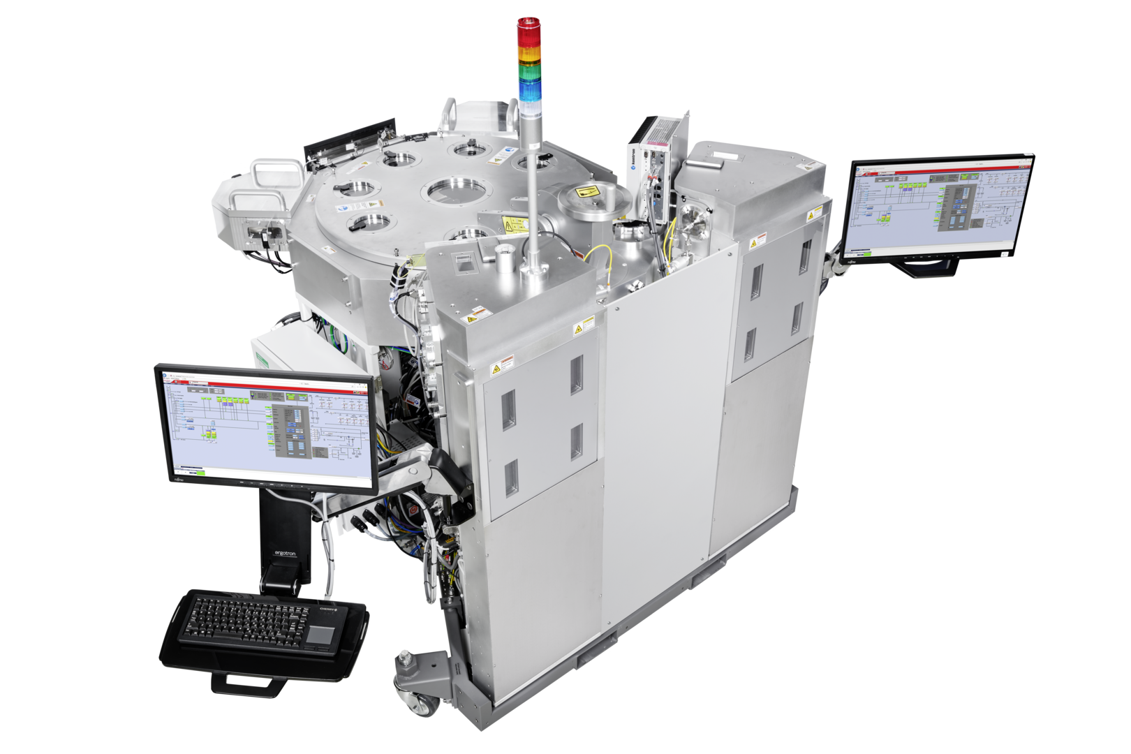
AIXTRON has secured an order from US semiconductor developer Aeluma for a G10-AsP metalorganic chemical vapour deposition system, supporting the expansion of photonic device manufacturing using larger gallium arsenide and silicon substrates.
Aeluma confirmed the purchase agreement on 12 November. The equipment supports 150 mm and 200 mm wafers and has been specifically configured for the company’s non-indium-phosphide photonics platform. It will be used for further process development and the expansion of manufacturing capability for photodetectors and lasers.
The order extends an existing collaboration between the companies as Aeluma develops semiconductor technologies intended to increase the manufacturing scale of optical components. Its approach combines selected compound semiconductor materials with microelectronics-grade gallium arsenide or silicon substrates, providing an alternative to conventional production based on indium phosphide wafers.
High-speed optical components are becoming increasingly important within computing infrastructure. AI systems require large volumes of information to move between processors, accelerators, networking equipment, and other devices. As electrical interconnects encounter bandwidth, power, and distance constraints, optical transmission provides an alternative for suitable parts of the communications architecture.
Photodetectors convert received optical signals into electrical information, while semiconductor lasers provide the light used in many optical transmission systems. Their electrical and optical characteristics depend on the semiconductor materials, device structures, and fabrication processes used during production.
Indium phosphide has an established role in high-performance photonics because its material properties support optical devices used in communication systems. However, substrate availability, wafer dimensions, and manufacturing economics can complicate efforts to increase production volumes.
Aeluma’s technology is designed to address part of this constraint by integrating compound semiconductor materials with larger substrates commonly associated with microelectronics manufacturing. The approach seeks to retain the optical properties required by specialised devices while allowing production to expand using wafer formats and processing methods suitable for greater manufacturing scale.
The G10-AsP system provides the epitaxial growth capability needed for this approach. Metalorganic chemical vapour deposition, or MOCVD, introduces chemical precursors into a controlled reactor environment, where they react at the heated wafer surface to form semiconductor layers.
Those layers must meet demanding specifications for thickness, composition, and interface quality. Small variations can affect the electrical and optical behaviour of the finished device, making process uniformity an important factor in semiconductor manufacturing yield.
Moving towards larger wafers also increases the area over which the deposition process must remain consistent. Temperature distribution, precursor delivery, reactor conditions, and contamination control influence the uniformity of the resulting material. Greater wafer area can increase the number of potential devices produced in one run, although that benefit depends on usable yield and the size of individual components.
AIXTRON has configured the G10-AsP specifically for Aeluma’s proprietary processes. The system is designed for automated, high-throughput manufacturing and supports both 150 mm and 200 mm substrate formats. The equipment’s stated capabilities establish the intended wafer sizes, but neither company has disclosed the planned number of wafers processed per production run or the expected manufacturing yield.
Process development remains important because semiconductor material growth is only one part of photonic device production. Epitaxial wafers must subsequently undergo fabrication steps to define device structures, electrical contacts, and optical features before the completed components can be tested and packaged.
Laser manufacturing introduces additional requirements involving optical confinement, material defects, electrical injection, and thermal behaviour. Photodetectors must similarly achieve the necessary sensitivity, response speed, and electrical characteristics for their intended operating conditions.
Meeting those requirements consistently across larger substrates depends on the combined performance of the deposition process and subsequent manufacturing operations. A larger wafer format does not automatically produce lower component costs if variations in material quality or later fabrication steps reduce the proportion of usable devices.
Aeluma is developing high-speed photodetectors, quantum dot lasers, and other photonic components for data communications. Its platform is intended to support optical technologies used within AI infrastructure, where increasing data throughput creates demand for components capable of operating at high speeds and in compact assemblies.
Quantum dot laser structures offer a different approach to controlling the active light-emitting region of a semiconductor device. Their performance depends on the characteristics of the semiconductor nanostructures and the surrounding device architecture, making material growth and process repeatability important areas of development.
Aeluma was established in 2019 as a spin-off from the University of California, Santa Barbara. Based in Goleta, California, it operates facilities for semiconductor wafer production, prototyping, device fabrication, testing, and validation. It also works with manufacturing and packaging partners as it develops commercial applications for its technology.
The latest equipment order represents a manufacturing investment rather than confirmation that the expanded capacity is already operating. Installation, process transfer, qualification, and subsequent production testing will determine when the system can contribute to additional commercial output.
Neither company has disclosed the purchase value, a confirmed delivery date, or a timetable for full production qualification. Those details remain relevant to assessing the scale and timing of the expansion.
The G10-AsP purchase provides Aeluma with a defined route towards larger-substrate photonics manufacturing. Its contribution to production volumes will depend on the qualification of the customised epitaxial processes and their integration with the remaining fabrication, packaging, and test operations.