IN Brief:
- Samsung has begun constructing a new HBM packaging facility at its Onyang semiconductor campus in Asan.
- The project involves ₩6 trillion in construction investment, with approximately ₩40 trillion planned for advanced equipment across the wider programme.
- The three-storey facility will contain 31,000 square metres of cleanroom space and is scheduled to begin operating in June 2028.
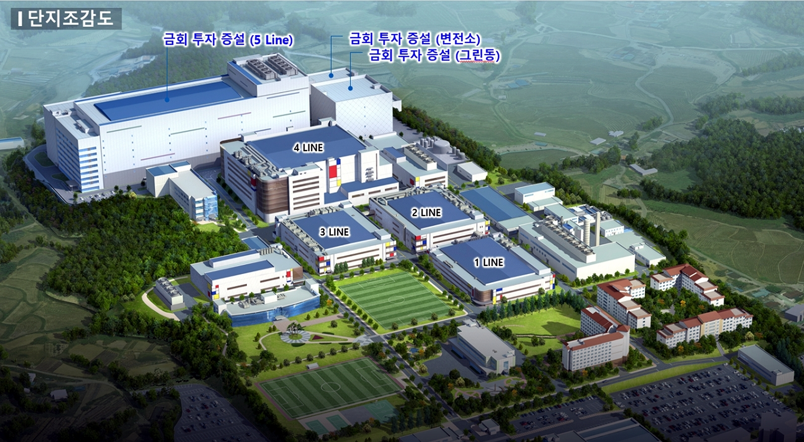
Samsung Electronics has begun construction of an advanced high-bandwidth memory packaging facility at its Onyang semiconductor campus in Asan, South Korea, expanding manufacturing capacity for memory devices used alongside high-performance processors and AI accelerators.
The new production line is scheduled to begin operating in June 2028, approximately one year earlier than the previously reported timetable. Construction commenced on 12 November during a ceremony attended by Samsung Electronics Chairman Lee Jae-yong and South Korean President Lee Jae-myung.
Samsung plans approximately ₩46 trillion in investment across a wider programme involving five HBM production lines at the campus. The expenditure comprises ₩6 trillion associated with construction and approximately ₩40 trillion in advanced manufacturing equipment to be installed in phases.
The distinction between these figures is important. The ₩46 trillion represents the broader investment programme rather than the construction cost of the single facility now under development. Equipment spending will also occur over time as the campus expansion progresses.
The new facility will provide approximately 31,000 square metres of cleanroom space across three floors. When the wider development is completed, the campus is expected to have approximately 420,000 square metres of floor space, compared with around 270,000 square metres currently.
Samsung’s Onyang operation began as a semiconductor assembly and testing facility in 1991. Its expansion into advanced memory packaging reflects the increasing complexity of integrating memory and processing devices within high-performance computing systems.
High-bandwidth memory differs from conventional memory arrangements by combining multiple DRAM dies in vertically integrated stacks. The structure allows a large number of electrical connections to be accommodated within a comparatively compact package, supporting high data transfer rates between memory and associated computing hardware.
Through-silicon vias provide electrical pathways through individual semiconductor dies, allowing signals and power to move between layers. Additional interconnect and bonding processes join those structures into an assembly that must maintain electrical continuity and mechanical reliability during operation.
After the memory stack has been produced, it is typically integrated into a larger package containing a processor or accelerator. The short, dense connections between memory and processing hardware provide the bandwidth required by demanding computing applications.
AI accelerators depend heavily on memory performance because processing units must continuously access model parameters and intermediate calculation results. Increasing arithmetic capability without sufficient memory capacity and bandwidth can leave part of the processor’s available computing performance unused.
HBM addresses this constraint through close physical integration and a wide memory interface. Its manufacture, however, introduces production requirements beyond those associated with conventional semiconductor memory devices.
Each additional die creates more interfaces that must function correctly. Wafer thinning, alignment, bonding, interconnect formation, and testing must be controlled to prevent defects from compromising the completed memory assembly.
The relationship between component yield and finished product yield becomes particularly important in stacked devices. A defective die or interconnect can affect an assembly containing several otherwise functional components, increasing the cost of manufacturing losses.
Advanced inspection and testing are consequently important throughout production. Manufacturers must verify electrical continuity, identify defective structures, and assess the reliability of assembled devices before they proceed into more expensive packaging stages.
Thermal management presents another challenge. Stacked memory dies generate heat during operation, while their proximity to high-performance processors can introduce additional thermal demands. Material selection, package construction, and the cooling arrangement of the finished computing system influence operating temperature and long-term reliability.
Increasing HBM output therefore requires coordinated investment in memory fabrication and advanced packaging. Additional DRAM wafer capacity cannot automatically produce more completed HBM devices if stacking, bonding, testing, or integration operations remain constrained.
The new Onyang facility addresses part of that manufacturing requirement. Its planned cleanroom space will accommodate specialised equipment associated with advanced memory packaging, although Samsung has not published a detailed allocation of individual equipment types or their intended production capacities.
Bringing the facility into operation will require installation, commissioning, process qualification, and production testing. The June 2028 target describes the planned beginning of operations and does not establish that every production line will be operating at full capacity at that date.
The expansion forms part of a wider programme of industrial investment in South Korea’s Chungcheong region. Samsung affiliates are also developing semiconductor substrates, displays, and other advanced manufacturing facilities, supported by government measures intended to accelerate construction and industrial infrastructure development.
Electrical supply, water availability, transport infrastructure, and environmental approvals are important considerations for semiconductor expansion projects. The South Korean government has outlined additional support for major developments in the region, including measures concerning industrial utilities, permitting, and associated suppliers.
Samsung expects the Onyang development to create approximately 700 direct jobs. The company has not disclosed a detailed monthly HBM output target for the new facility or the specific memory generations to be allocated to each production line.
The manufacturing expansion takes place amid continuing demand for advanced memory used in AI servers. Samsung has indicated that negotiations over its planned 2027 HBM supply volumes have been completed, although customers continue to request additional shipments.
Those commercial discussions do not establish the output that will eventually be achieved at Onyang. Production capacity depends on the installation and qualification of equipment, the availability of suitable semiconductor materials, and the yields achieved during manufacturing.
The reported acceleration of the operating timetable also remains subject to the practical constraints of a major semiconductor construction programme. Completion of the building, installation of advanced equipment, and successful process qualification are separate milestones.
The Onyang project establishes a substantial manufacturing commitment behind Samsung’s HBM expansion. The June 2028 operating target, equipment investment phases, and subsequent production qualifications will determine when the new capacity can begin contributing to commercial memory supply.