IN Brief:
- Besi is joining Applied Materials’ EPIC Center as an Innovation Partner, extending collaboration established around hybrid bonding in 2020.
- Planned R&D covers thermo-compression bonding, several die integration formats, and photonics-enabled interconnects alongside new hybrid bonding platforms.
- The expanded programme builds on the companies’ Singapore development centre and their jointly developed Kinex die-to-wafer bonding system.
Applied Materials and BE Semiconductor Industries, or Besi, are expanding their advanced packaging partnership, with Besi joining Applied’s EPIC Center as an Innovation Partner and extending joint development beyond the hybrid bonding work started in 2020.
The companies plan to work across new hybrid bonding platforms, thermo-compression bonding, die-on-wafer, die-on-die and die-on-panel integration, as well as photonics-enabled interconnects. Besi engineers will work alongside Applied teams at the Silicon Valley research centre, giving both companies a shared environment for process and assembly development.
The programme builds on the Hybrid Bonding Center of Excellence established by the companies in Singapore. That collaboration combined Applied’s work in areas including deposition, planarisation, cleaning, metrology, inspection and defect control with Besi’s die placement and assembly capability. It subsequently produced the Kinex integrated die-to-wafer hybrid bonding system.
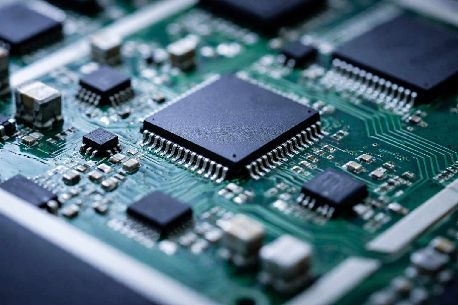
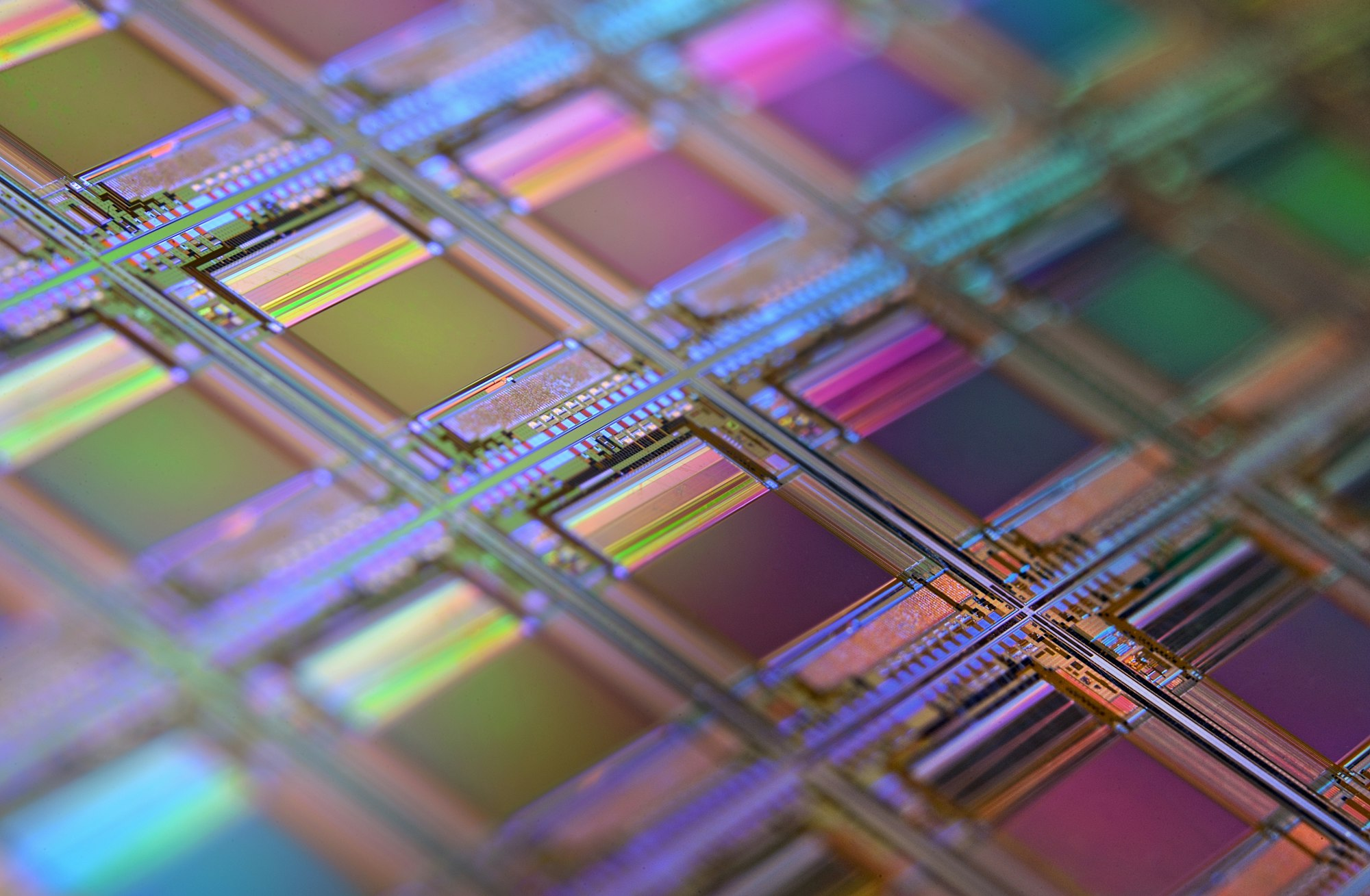
Hybrid bonding is becoming more prominent as semiconductor designs split large systems across multiple dies. Direct copper connections can increase interconnect density and shorten electrical paths between logic, memory and specialised accelerators, but they also tighten requirements around surface preparation, die alignment, cleanliness, planarity and defect control.
Those requirements increasingly connect processes that were once treated separately. Wafer preparation affects bonding quality, placement accuracy determines whether fine interconnect structures meet correctly, and contamination or surface variation can translate directly into package yield. Equipment suppliers therefore have to optimise several connected steps rather than treating bonding as an isolated back-end operation.
Thermo-compression bonding remains part of the expanded programme alongside hybrid bonding. The companies will also investigate die-on-panel and other integration formats, reflecting the wider range of package architectures being developed for AI and high-performance computing systems. Panel processing can increase the usable manufacturing area available during packaging, although it introduces separate challenges in warpage, handling and process uniformity.
Photonics adds another integration layer. Co-packaged optics places optical interfaces close to switching or compute silicon, which introduces alignment, thermal, assembly and test requirements alongside the electrical interconnect problem. Applied and Besi have not announced a resulting photonics product, but optical integration is explicitly included in the extended development scope.
Dr Prabu Raja, President of the Semiconductor Products Group at Applied Materials, said: “Advanced packaging is no longer a back-end assembly step – it is a materials engineering challenge.” The expanded programme follows that premise by combining wafer process technology and assembly development inside the same research environment.
Applied is building the EPIC Center as a shared semiconductor process development site, with its investment expected to scale to around $5 billion as customer programmes increase. Chipmakers, systems companies, universities and equipment suppliers are intended to work on connected manufacturing problems before transferring qualified processes into high-volume production.
Besi is simultaneously expanding its role in other advanced packaging programmes. The company has also agreed to support Tata Electronics’ advanced packaging operation in India, covering equipment, process readiness and engineering capability for the Jagiroad semiconductor assembly facility.
The Applied partnership has a different structure, centred on joint process development rather than deployment at one customer factory. Applied contributes front-end materials engineering and process control, while Besi supplies die handling, alignment and assembly expertise. Their earlier collaboration established a route from research into a commercial bonding platform, providing a reference point for the broader programme now under way.
The next outputs are likely to emerge as equipment, process modules and integration methods rather than a single package architecture. Hybrid bonding, thermo-compression bonding, panel processing and photonics each impose different manufacturing constraints, and customers will ultimately select combinations according to interconnect density, thermal performance, die size, cost and production volume.
The partnership now covers a larger section of that manufacturing chain. Its progress will be measured by whether the shared development model can turn increasingly complex package structures into repeatable production processes while maintaining the alignment, cleanliness and yield demanded by semiconductor manufacturing.