IN Brief:
- Elephantech has made the first overseas shipment of its DK100 inkjet manufacturing system to a PCB producer.
- DeepVia HDI combines copper nanoink and precision inkjet deposition to metallise microvias with aspect ratios of 2.0 and above.
- The equipment is intended to enter a mass-production line making AI-server boards for a leading North American chipmaker.
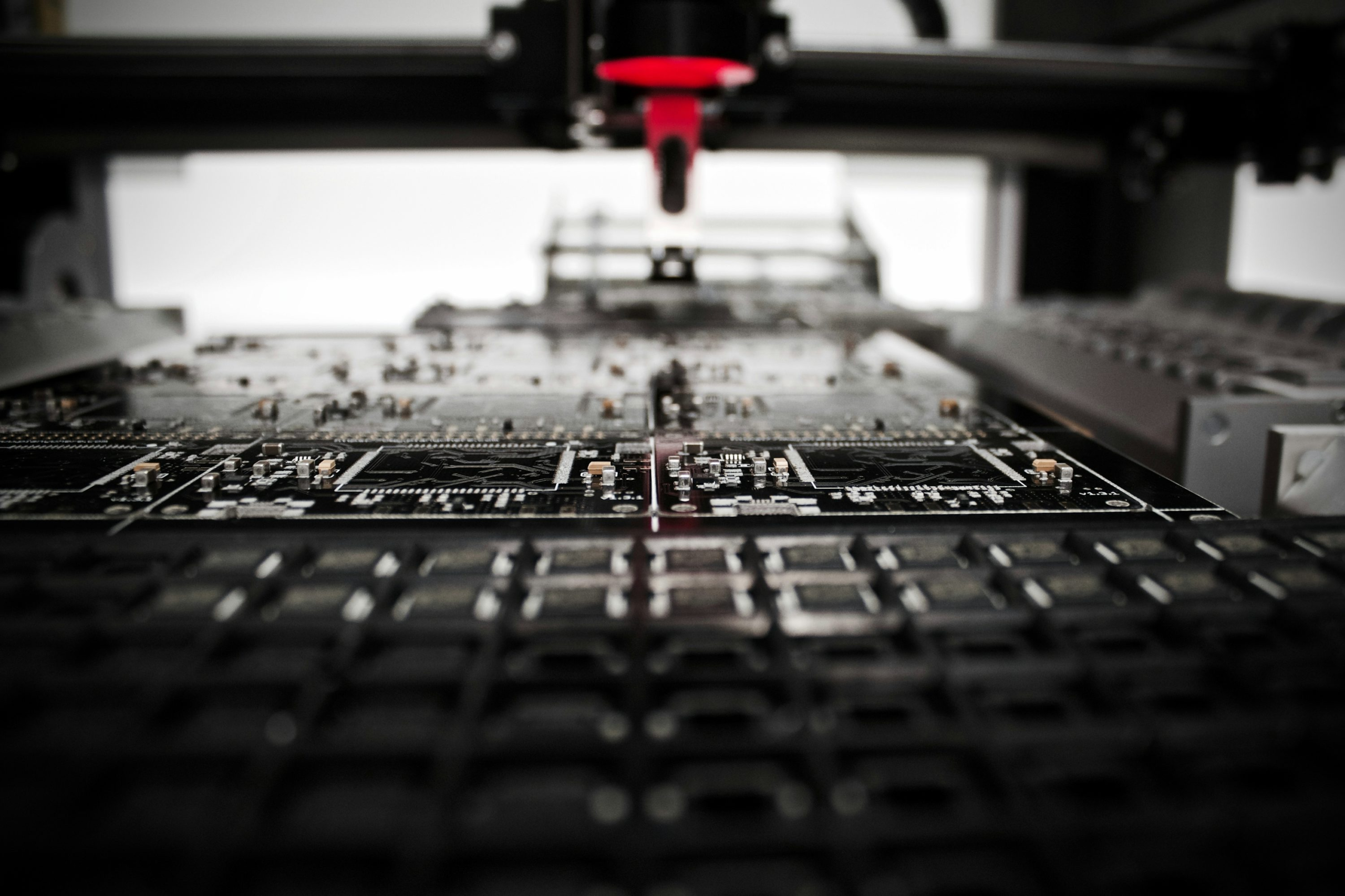
Elephantech has shipped its first DK100 inkjet manufacturing system overseas, moving the DeepVia HDI process from technology introduction towards use on a customer production line for high-density printed circuit boards.
The receiving PCB manufacturer plans to install the equipment on a line producing AI-server boards for a leading North American chipmaker. Neither company has been identified, and Elephantech has not published throughput, yield, cycle-time, or qualification figures for the installation, leaving the shipment as an industrialisation milestone rather than evidence of completed volume production.
DK100 uses copper nanoink with precision inkjet deposition to metallise high-aspect-ratio microvias. Elephantech specifies support for structures with aspect ratios of 2.0 and above, a geometry that becomes progressively harder to coat reliably as interconnect dimensions shrink and board constructions become thicker.
Microvias provide vertical connections between layers in high-density interconnect boards without consuming the area associated with larger mechanically drilled vias. Increasing the achievable aspect ratio can give designers more freedom over layer stacks and escape routing around dense packages, but deeper, narrower structures are more difficult to metallise without voids, uneven coverage, or weak interfaces.
Conventional PCB metallisation has to balance deposition uniformity, chemistry, process control, and increasingly aggressive via geometry. Inadequate coverage can raise electrical resistance, create reliability weaknesses, or reduce production yield. Elephantech’s approach instead deposits conductive nanoink selectively with an inkjet process, changing how copper is introduced into the microvia structure.
The manufacturing case will depend on more than the geometry demonstrated by the process. Print speed, curing conditions, adhesion, final conductivity, inspection requirements, panel utilisation, maintenance, and repeatability all influence whether the equipment can compete with established production methods. Elephantech has not yet disclosed those figures for the customer installation.
AI-server boards provide a demanding application. Accelerator and switching systems are driving higher layer counts, larger packages, dense memory interfaces, and faster serial links. Routing geometry, via stubs, insertion loss, impedance control, and transitions between package and board become increasingly restrictive as channel rates and interconnect density rise.
Board and package design tools are responding to the same constraints. Recent PCB and package automation development has increasingly treated layout, manufacturability, signal behaviour, and multiphysics effects as connected problems. A production process that changes the feasible microvia geometry can therefore affect routing decisions made well before a panel reaches fabrication.
Elephantech introduced DeepVia HDI in April and has moved to its first overseas equipment shipment around five months later. The DK100 sits alongside the company’s DS-SAP work for advanced semiconductor substrates, putting its copper deposition technology into two manufacturing areas being driven by high-performance computing hardware.
PCB processes face a considerable gap between materials demonstrations and stable factory operation. Production equipment has to maintain registration and deposition consistency across large panels, integrate with upstream and downstream process steps, tolerate maintenance cycles, and produce structures that survive the customer’s electrical and mechanical reliability testing.
The customer installation will now move DeepVia HDI into that environment. Production yield at the target microvia geometry, panel throughput, electrical resistance, thermal-cycle reliability, and the routing freedom achieved in finished boards will determine how much value the inkjet process adds over incumbent metallisation methods.
The first shipment therefore marks a change in maturity rather than proof of production performance. Elephantech has moved its process onto customer equipment; the next evidence will come from the stability and economics of the line once the DK100 is operating on AI-server PCB designs.