IN Brief:
- Co-packaged optics requires increasingly dense integration of photonic ICs, electronic ICs, lasers, optical structures, and thermal materials.
- EV Group is applying hybrid and fusion bonding, nanoimprint lithography, and thin-wafer processing to CPO manufacturing flows.
- Its Austrian competence centres support process development and validation before transfer into high-volume semiconductor manufacturing.
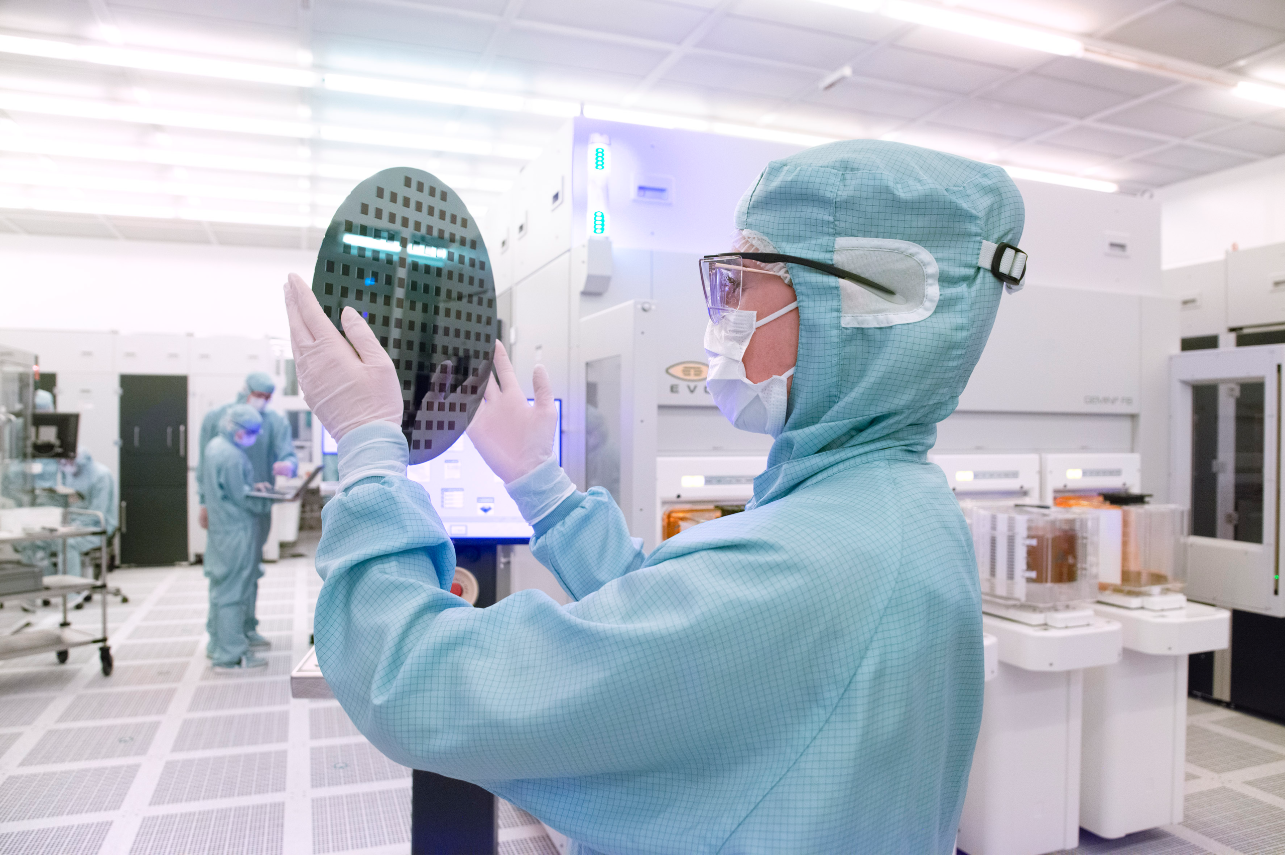
EV Group is extending its semiconductor process portfolio into co-packaged optics, combining wafer bonding, nanoimprint lithography, and thin-wafer processing to support increasingly dense integration of photonic and electronic components.
The Austrian equipment supplier is working with customers and partners across the CPO ecosystem as AI and high-performance computing systems place greater pressure on the electrical links between processors, switches, and optical transceivers. Moving optical I/O closer to the compute package can shorten those high-speed electrical paths, but it also brings photonic integrated circuits, electronic ICs, lasers, optical couplers, and thermal structures into a much tighter manufacturing envelope.
EV Group is addressing the integration problem through several established process technologies rather than a single dedicated CPO platform. Hybrid bonding can create low-parasitic connections between photonic and electronic integrated circuits, while fusion bonding supports heterogeneous material combinations used in laser fabrication and emerging modulation technologies.
The company is also applying oxide-free room-temperature bonding to low-loss optical interfaces and to the integration of heat-spreader materials including diamond and silicon carbide. Thermal management becomes increasingly closely coupled to the interconnect architecture as photonic and electronic devices are brought together inside the same package.
Different materials add another layer of process control. Silicon electronics, III-V semiconductor light sources, thin-film electro-optic materials, and optical structures have different surface, thermal, and mechanical properties, leaving bond quality, interface loss, alignment, and thermal expansion linked to the finished optical performance.
Nanoimprint lithography forms the second major part of EV Group’s CPO process offering. The technique can replicate grating couplers, vertical optical coupling structures, and beam-shaping elements used to move light between chips and fibres or out of the wafer plane. Production requires those structures to retain their geometry and alignment across large numbers of devices rather than merely demonstrate acceptable optical behaviour on individual prototypes.
Temporary bonding and debonding support wafer thinning for laser-diode fabrication and other advanced packaging processes. Those steps affect package thickness, thermal resistance, handling, and integration density, making them part of a common manufacturing sequence rather than isolated wafer-processing operations.
EV Group is supporting CPO development through its NILPhotonics Competence Center and Heterogeneous Integration Competence Center in Austria. The facilities allow customers to develop and validate processes in a production-relevant environment before transferring them to high-volume manufacturing. EV Group’s 1 September announcement explicitly positions that transfer step as part of its CPO work.
Manufacturing flexibility is likely to remain necessary because the industry has not settled on one CPO architecture. Light sources may be integrated or external, optical engines can be arranged differently around the switching or compute device, and future designs are expected to extend into optical I/O chiplets and more complex three-dimensional photonic-electronic integration.
That development increases the number of process interfaces that must remain repeatable at semiconductor manufacturing scale. Bond alignment, optical coupling, die placement, wafer thinning, heat transfer, and packaging yield all have to work together before the bandwidth advantages of CPO can be realised economically.
EV Group’s approach is therefore rooted in process integration rather than a single optical component. Hybrid and fusion bonding address heterogeneous device stacks, nanoimprint lithography provides repeatable optical structures, and thin-wafer techniques support the physical assembly. The commercial test will be whether those processes can maintain optical performance and yield as CPO moves from specialist development programmes into larger-volume compute infrastructure.