IN Brief:
- imec’s Ge/Si avalanche photodiode combines 100GHz bandwidth, 5V operation and 1.8A/W responsivity across the O- and C-bands.
- The detector delivered a 3dB receiver-sensitivity improvement in a net 400Gbps optical link fabricated on imec’s 300mm silicon photonics platform.
- Further development will focus on reliability across wider operating conditions and integration with high-speed receiver electronics.
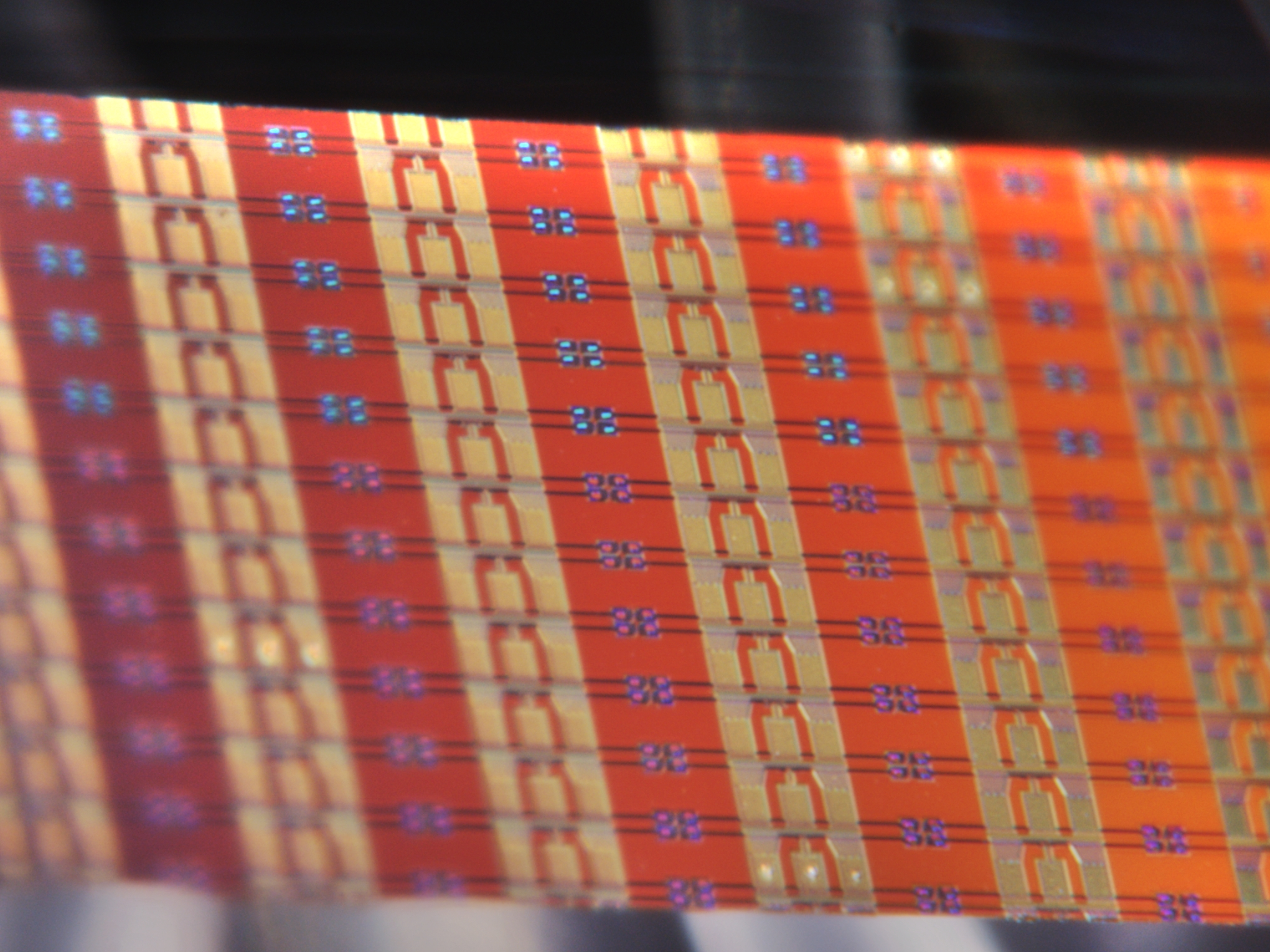
imec has demonstrated a net 400Gbps optical link using a germanium-on-silicon avalanche photodiode combining 100GHz bandwidth, 5V operation and 1.8A/W responsivity. Fabricated on the research organisation’s 300mm silicon photonics platform, the detector delivered a 3dB improvement in receiver sensitivity while operating across both the O- and C-bands.
Avalanche photodiodes use internal multiplication to amplify an incoming optical signal before it reaches the receiver electronics. The additional gain can improve sensitivity, but conventional APD designs often trade bandwidth against bias voltage and multiplication performance. imec’s development targets that compromise with a Ge/Si structure able to maintain high bandwidth while operating at a voltage compatible with more compact receiver architectures.
The device uses a separate absorption, charge and multiplication architecture, with imec scaling the multiplication region to below 100nm. A deeply recessed germanium-in-silicon structure is combined with removal of the conventional charge layer, resulting in roughly twofold internal gain while preserving the quoted 100GHz bandwidth at 5V.
Comparable O- and C-band performance also gives optical-system designers more freedom over wavelength selection. O-band links are widely used for short-reach datacentre connectivity because silicon photonics components and fibre dispersion are well suited to the wavelength range, while C-band operation opens further options around wavelength multiplexing and longer optical paths.
For the 400Gbps demonstration, imec paired the APD with the beyond-110GHz C-band Ge/Si electro-absorption modulator it disclosed at ECOC 2025. Combining a high-speed transmitter and internally amplified receiver in the same link moves the work beyond a standalone detector measurement and provides a clearer indication of how the component behaves within a complete optical channel.
The 3dB sensitivity improvement creates additional optical link margin. System designers can use that margin to absorb losses through couplers, fibres and packaging interfaces, or reduce the optical power needed to maintain the required bit-error performance. Both approaches are relevant as optical interfaces become denser and move closer to switches, accelerators and other high-bandwidth silicon.
AI systems are increasing the amount of data exchanged between accelerators, switches and racks while electrical reach becomes progressively more expensive in power and signal-conditioning terms. Equalisation, retimers and high-speed SerDes circuitry can maintain electrical performance, but the power penalty grows as lane rates rise. Silicon photonics is consequently moving deeper into scale-up and scale-out architectures, placing greater pressure on the efficiency of every optical component in the link.
Receiver operating voltage also affects the surrounding electronics. Large APD bias supplies add complexity to power delivery and can make integration with transimpedance amplifiers and other receiver circuitry more difficult. A 5V detector does not remove those system constraints, but it narrows the gap between internally amplified photodetection and the supply environment expected around densely integrated optical modules.
Fabrication on imec’s iSiPP300 300mm platform gives the work a manufacturing route beyond small-scale photonic test structures. Larger wafers support greater device volumes and closer process control, while the common platform allows modulators, detectors and passive photonic structures to be developed within a repeatable silicon manufacturing flow. Packaging, thermal behaviour and long-term reliability will still determine whether the detector can make the transition into deployed hardware.
imec’s next steps include broader reliability testing across temperature and optical input-power ranges, followed by integration with high-speed receiver electronics. That stage will expose the APD to the parasitics, noise and bandwidth limitations of a complete receiver chain. The current link demonstration establishes that internal optical gain, 100GHz bandwidth and low-voltage operation can coexist on a 300mm silicon photonics platform at net 400Gbps data rates.