IN Brief:
- Tenth-generation BiCS Flash combines a 332-layer NAND array with separately manufactured CMOS circuitry.
- Initial 1Tb TLC devices support a NAND interface speed of 4.8Gb/s.
- Kioxia is targeting enterprise and data-centre storage used in AI infrastructure.
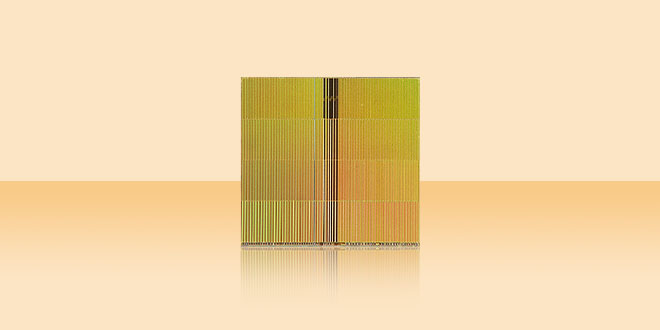
Kioxia has begun sampling tenth-generation BiCS Flash devices built around a 332-layer three-dimensional NAND structure. The initial 1Tb triple-level-cell memory targets enterprise and data-centre solid-state drives used for AI training, inference, retrieval, and large-scale data processing.
Production will use Kioxia’s Kitakami Fab2 in Japan and a process that manufactures the memory array and CMOS control circuitry on separate wafers before bonding them directly. That separation allows each wafer to be optimised for its own electrical and process requirements rather than forcing both structures through one combined manufacturing flow.
An on-pitch select-gate-drain layout increases array efficiency, while the additional layers and revised architecture raise bit density by 59% against the eighth generation. The NAND interface reaches 4.8Gb/s, 33% higher than the earlier generation, with improved power efficiency during both read and write operation.
Although the component figures are substantial, they do not describe the performance of a finished SSD. Controller design, error correction, channel count, firmware, over-provisioning, thermal management, host interface, and workload shape the capacity and sustained performance delivered by a complete drive.
Direct wafer bonding has become an important route for scaling three-dimensional NAND because peripheral circuitry can be developed independently from the memory stack. It also introduces exacting requirements around alignment, surface preparation, wafer bow, contamination, bond integrity, and yield.
A fault discovered after bonding can compromise valuable circuitry on both wafers, making process control as important as nominal layer count. Taller stacks also increase the difficulty of etching deep, uniform channels and maintaining electrical behaviour from the top of the array to the bottom.
Kioxia is pursuing a dual-axis strategy rather than moving every product immediately to the highest layer count. Ninth-generation BiCS Flash emphasises performance and capital efficiency, while the tenth generation pushes density and interface capability for markets able to absorb the newer process.
Because storage markets carry widely different priorities, that distinction allows process choices to follow application requirements. Industrial and embedded products may favour endurance, controlled change, temperature range, and long availability, whereas enterprise systems place greater weight on capacity, throughput, power per stored bit, and rack-level operating cost.
AI infrastructure has expanded demand for persistent storage alongside the more visible requirement for high-bandwidth DRAM. Training sets, checkpoints, model weights, vector databases, and retrieval systems all occupy NAND, while inference services need large data collections to remain available with predictable latency.
As demand returns, capital spending is following it across both DRAM and three-dimensional NAND production. Forecasts that memory-equipment investment will pass $50 billion show how the sector is drawing renewed expenditure after an extended period of caution and inventory correction.
Even as NAND interfaces accelerate, they cannot remove every bottleneck within a complete storage path. SSD controllers must manage stronger error correction, more parallel channels, power-loss protection, thermal limits, and increasingly fast PCIe links, while host boards need sufficient lanes, signal integrity, cooling, and software capable of sustaining parallel I/O.
Power efficiency may be as commercially significant as raw interface speed because small reductions at die level accumulate across thousands of drives. Greater density can lower the number of packages needed for a target capacity, although concentrating more data in each package raises the operational consequence of a device failure.
Read latency and quality-of-service behaviour will also be scrutinised once the parts enter full SSD designs. AI data pipelines can generate highly variable access patterns, so peak transfer figures must be considered beside tail latency, thermal throttling, garbage collection, and recovery after background media-management activity.
The company’s PCIe 5.0 BG8 family uses eighth-generation BiCS Flash in compact client drives, whereas the tenth-generation sampling programme begins with enterprise priorities. Product qualification will determine when the new memory moves into complete drives and how broadly it spreads across the portfolio.
Controller and SSD manufacturers can now begin electrical characterisation, firmware development, error-management work, and reliability testing with sampled devices. Volume adoption will rest on yield progression at Kitakami Fab2 and on whether the bonded architecture maintains endurance and predictable performance under sustained data-centre workloads.