IN Brief:
- L&T Semiconductor and Tata Electronics will explore fabrication and packaging routes for L&T-designed semiconductor products.
- Engineering work will include design-to-fabrication optimisation intended to improve manufacturability and production scale.
- Target markets include automotive, industrial, communications, security, and intelligent-edge systems.
L&T Semiconductor Technologies and Tata Electronics have agreed to explore domestic fabrication and packaging routes for L&T-designed chips, creating a potential path from fabless product development into Indian wafer production and back-end manufacturing.
The partnership covers current and future semiconductor products and will assess Tata Electronics’ foundry process technologies and packaging solutions against L&T Semiconductor’s device portfolio. The companies also plan design-to-fabrication optimisation work intended to improve manufacturability as products move from design databases towards volume production.
That engineering work goes beyond a straightforward capacity reservation. Foundry migration requires a design to match the electrical rules, device models, process options, physical-design constraints, reliability requirements, and manufacturing tolerances of the selected process. Package selection adds another set of thermal, electrical, mechanical, and test constraints.
L&T Semiconductor is building a fabless portfolio across power devices, compute, analogue and mixed-signal products, IoT modules, and RF components. Its intended application markets include automotive, industrial equipment, energy systems, data centres, and telecommunications, giving the Tata relationship scope to span substantially different process and packaging requirements.
There is no single manufacturing flow suited to every part of that portfolio. High-voltage power devices, mixed-signal controllers, secure devices, RF products, and digital compute silicon each place different demands on transistor structures, passive components, metallisation, packaging, qualification, and test.
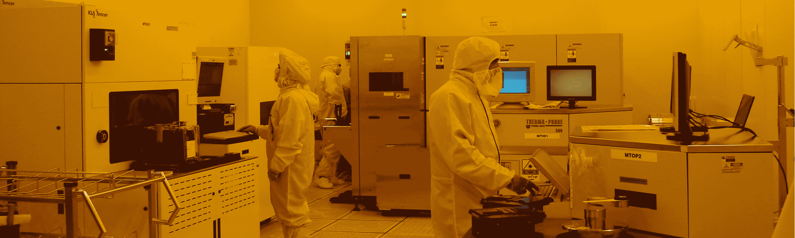
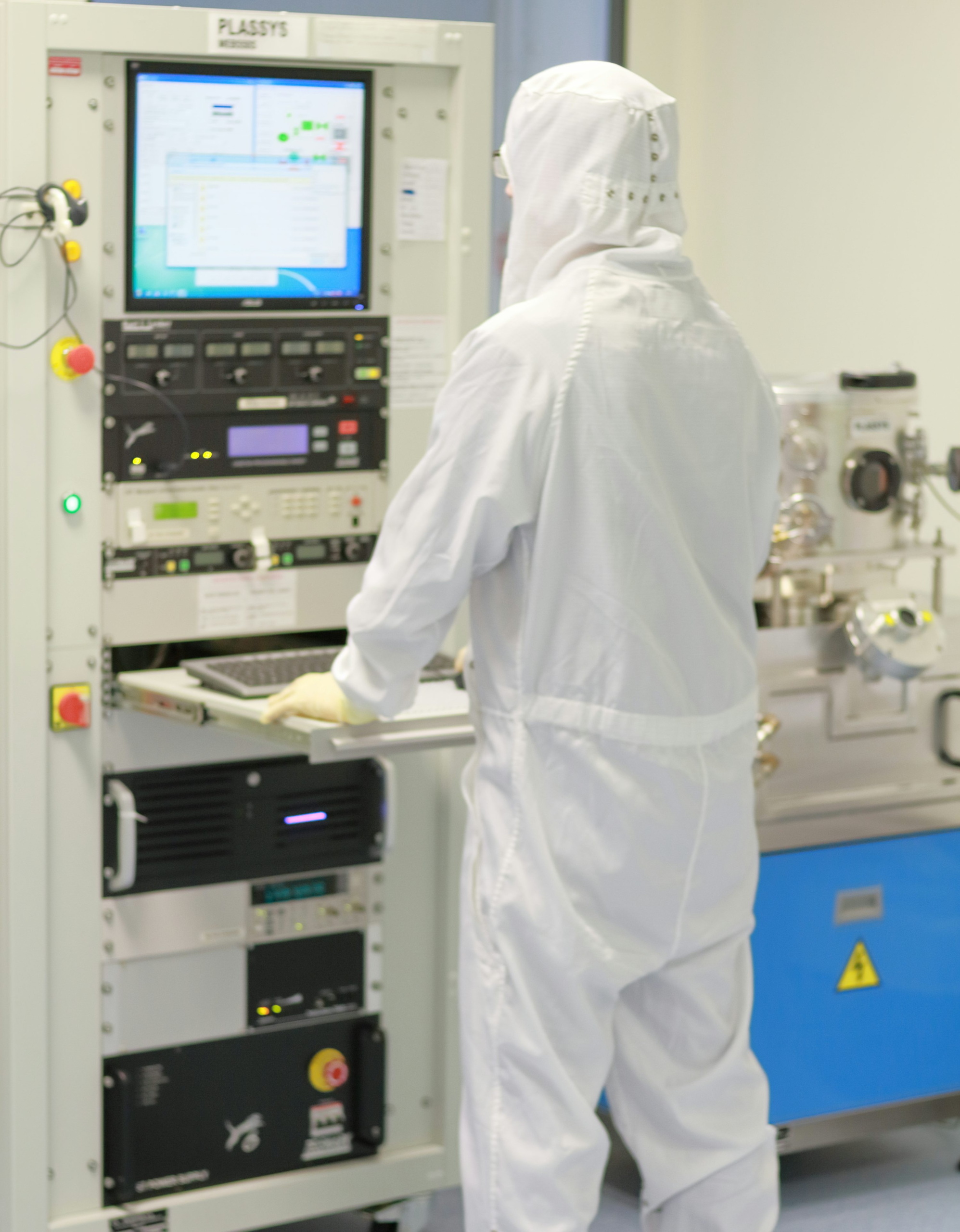
Tata Electronics is developing both front-end and back-end manufacturing capability. Its Dholera project is a planned 300mm foundry, while the Jagiroad operation in Assam is being built around semiconductor assembly and test. Linking both operations to a domestic fabless supplier could create a more continuous product-development path rather than routing design, wafer production, and packaging through unrelated suppliers.
The agreement remains exploratory. Neither company has identified a particular L&T device committed to a Tata process, and no process node, package family, tape-out date, qualification schedule, or volume-production date has been disclosed. The announcement therefore establishes a manufacturing framework rather than a confirmed production award.
The agreement sits among a rapid sequence of Tata Electronics agreements. Recent Nexperia and Tata manufacturing plans are more specific, covering planned 300mm MOSFET manufacturing at Dholera and assembly and test at Jagiroad. A separate Besi agreement addresses advanced packaging equipment and process capability at Jagiroad.
The L&T relationship sits further upstream by examining how a domestic chip designer could use Tata’s manufacturing stack. If individual devices progress, the useful engineering markers will be process selection, design-kit availability, test-chip or tape-out activity, package definition, reliability qualification, and first production silicon. A concrete manufacturing step would also show which parts of L&T’s portfolio can use Tata’s initial process offering without redesign or an alternative foundry route.
Design-for-manufacturing work becomes more important as devices and packages grow in complexity. A layout can be electrically correct yet still produce poor yield if it operates too close to process limits or creates difficult patterning, density, thermal, or packaging conditions. Early collaboration between designers and manufacturing engineers can expose those problems before masks and qualification make changes more expensive.
The same principle applies to packaging. Power devices may prioritise thermal resistance and current handling, RF parts have to control parasitics, and high-density digital silicon increasingly depends on package interconnect as part of system performance. Treating packaging as an early design variable rather than a final assembly choice can reduce later engineering iterations.
L&T Semiconductor and Tata Electronics identify automotive, industrial, communications, security, and intelligent-edge systems among the intended markets. Several of those sectors also bring long product lifetimes and qualification requirements, increasing the importance of supply continuity, process stability, and documented manufacturing change control.
For now, the agreement establishes the engineering route rather than production volume. Its progress will become measurable when an identified L&T design reaches a named Tata process and moves through tape-out, packaging, qualification, and customer availability.