IN Brief:
- Mitutoyo has established a dedicated Semiconductor Competence Center in Dresden within the Silicon Saxony microelectronics cluster.
- The facility focuses on high-precision measurement and inspection for semiconductor manufacturing, including nanometre-level applications.
- Customers and industry partners will use the centre for applications work, training and technical collaboration around semiconductor metrology.
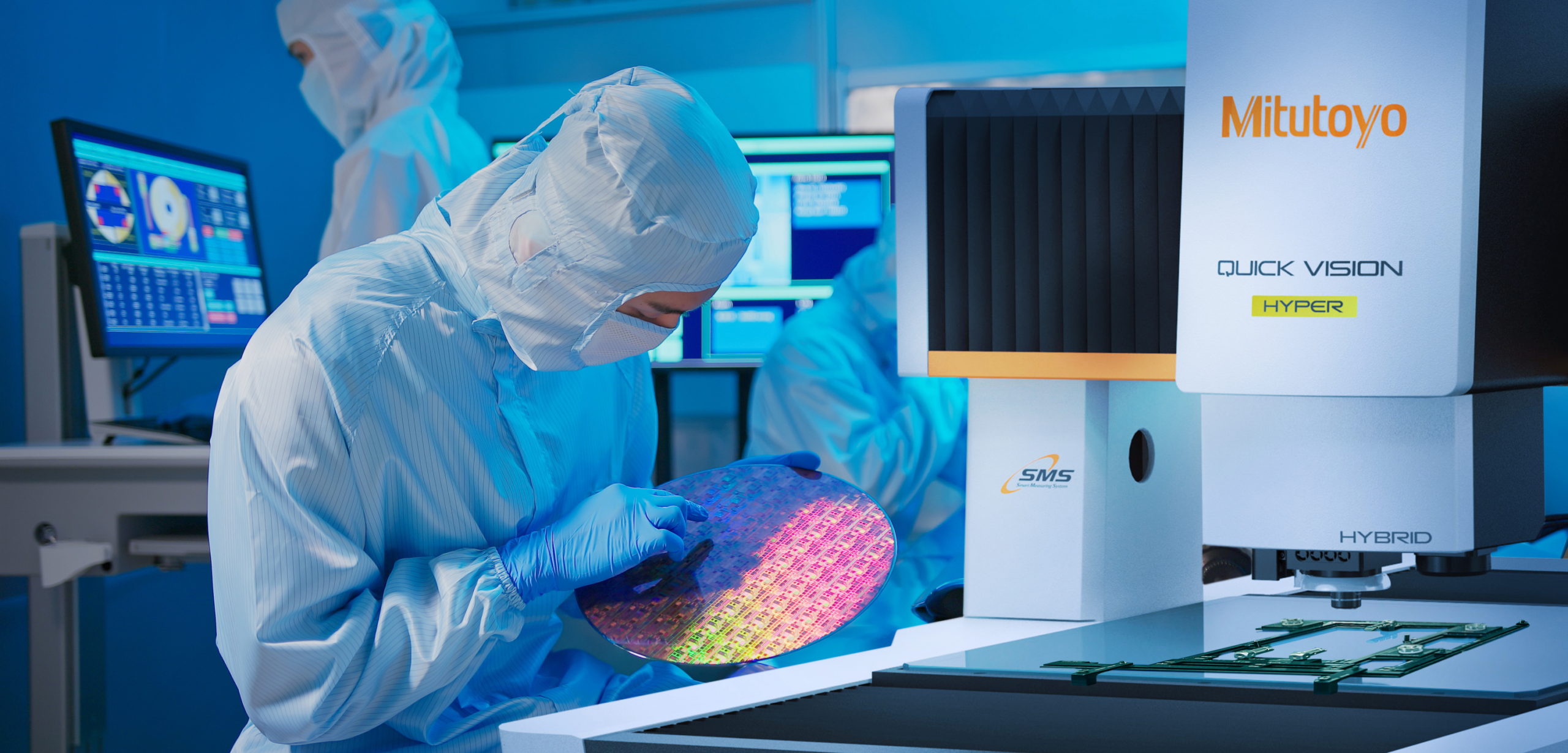
Mitutoyo has opened a Semiconductor Competence Center in Dresden, Germany, expanding its precision measurement and applications-support capability inside the Silicon Saxony microelectronics cluster. The facility is intended to support semiconductor manufacturers, equipment suppliers and technology partners as dimensional tolerances and inspection requirements become tighter across chip production.
The centre combines precision measurement equipment with semiconductor-specific applications expertise, including work at nanometre scale. Mitutoyo says its capabilities address dimensional accuracy, surface characteristics and geometric precision in processes where measurement uncertainty can affect quality, stability and manufacturing yield.
Metrology requirements are becoming more demanding as semiconductor structures shrink and packaging grows more complex. Measurements that were once associated mainly with wafer fabrication increasingly extend into advanced packaging, substrates, precision equipment parts and production tooling. Small dimensional errors can accumulate across several process stages, making reliable measurement central to controlling the complete manufacturing chain.
The Dresden centre is intended as an applications environment rather than simply a product showroom. Customers will be able to assess measurement methods against specific manufacturing problems, while Mitutoyo specialists provide support around instrument selection, measurement strategy and practical implementation.
Training and technical collaboration form another part of the facility’s remit. Semiconductor measurement cannot be reduced to selecting an instrument with sufficiently high stated resolution; fixturing, environmental stability, calibration, surface condition, measurement force and the geometry of the feature all affect the result.
At nanometre scales, temperature variation and vibration that would be insignificant in conventional mechanical measurement can become meaningful sources of uncertainty. Application support therefore becomes particularly important when semiconductor manufacturers transfer a laboratory measurement into a production environment that has to operate repeatedly across shifts, tools and product lots.
Dresden places that expertise inside one of Europe’s largest semiconductor manufacturing concentrations. Silicon Saxony brings together wafer manufacturers, equipment suppliers, research institutes, materials companies and electronics businesses, while continued regional investment is increasing demand for process-control and production-support technology.
Locating applications specialists close to those customers shortens the route between a manufacturing problem and practical measurement trials. It also gives equipment and process-development teams a local environment in which to compare approaches before measurement hardware is committed to a production line.
The centre reflects the wider role of precision mechanical metrology within semiconductor manufacturing. Lithography and electrical test attract much of the attention around chip production, but fabs and equipment manufacturers also depend on dimensional control across stages, fixtures, wafer-handling systems, optics, precision assemblies and production tooling.
Advanced packaging adds another set of requirements around substrates, package planarity and dense interconnect structures. As chiplets and heterogeneous integration place more devices inside one package, dimensional variation across those elements can have electrical, thermal and assembly consequences long before final electrical test identifies a problem.
Mitutoyo says the Dresden investment forms part of its longer-term commitment to semiconductor manufacturing in Europe and internationally. The company already supplies dimensional and optical measurement systems across manufacturing sectors, but a dedicated semiconductor centre gives it a location where those technologies can be developed around chip-production requirements rather than treated as general precision-engineering applications.
An open house is scheduled for 15 October 2026, giving customers, partners and industry representatives access to the facility and its measurement specialists. The broader significance, however, lies in the support ecosystem around European semiconductor expansion: additional fab capacity increases demand for metrology, test, materials, maintenance and engineering expertise alongside the wafer-processing equipment itself.
Mitutoyo’s Dresden centre adds another specialised capability to that infrastructure. As semiconductor investment expands across Silicon Saxony, proving that increasingly precise manufacturing processes are actually producing parts within specification will remain one of the less visible but unavoidable requirements of higher-volume European chip production.