
IN Brief:
- An existing Asian customer has ordered an SLX system for delivery during the second quarter of 2027.
- Laser-written photomasks remain central to production across mature semiconductor process nodes.
- Successive SLX orders point to sustained investment in mask capacity and equipment modernisation.
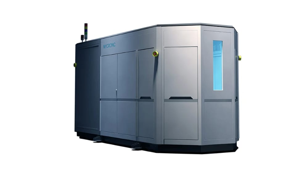
Mycronic has received an order valued between $5m and $7m for an SLX semiconductor photomask writer from an existing customer in Asia, with delivery scheduled for the second quarter of 2027.
The Swedish equipment manufacturer developed SLX to replace ageing laser mask writers and add capacity for photomasks used in semiconductor production. The platform shares technology with Mycronic’s display-mask systems but is configured for semiconductor masks and their associated throughput, registration, and critical-dimension requirements.
Photomasks carry the geometric patterns transferred onto wafers during lithography, with each device layer requiring its own controlled pattern. Mask quality and availability therefore sit at the beginning of the fabrication chain, where defects, dimensional variation, or registration errors can be reproduced across large numbers of devices before they appear in downstream test data.
Laser writing remains widely used for masks serving mature and less geometrically demanding nodes. Mycronic estimates that laser systems produce around 70% to 75% of semiconductor photomasks, reflecting their exposure economics and suitability for analogue, power, sensor, microcontroller, display-driver, and industrial products.
The latest order follows several SLX bookings during June, including systems for existing Asian customers and a new European customer. Taken together, the awards point to replacement of older equipment alongside capacity additions for the diverse product families manufactured on mature process geometries.
Mature nodes remain central to complete electronic systems even as advanced logic receives most investment attention. Vehicles, industrial controls, medical equipment, power systems, communications infrastructure, and sensors combine high-performance processors with much larger numbers of analogue, mixed-signal, power, interface, and control devices fabricated on established processes.
Design diversity can therefore increase even when leading-edge wafer volumes attract the largest individual factories. Every new microcontroller derivative, power-management device, sensor interface, or application-specific analogue component creates mask requirements, while established products need replacement masks and continuing production support throughout long commercial lives.
Equipment demand across the wider manufacturing chain is also strengthening. Global semiconductor equipment sales are forecast to approach $229bn by 2028, supported by AI infrastructure, memory investment, regional capacity expansion, advanced packaging, and continuing demand for power and analogue devices.
Photomask equipment occupies a specialised but critical position within that cycle. A wafer fab can add lithography, deposition, etch, metrology, and inspection capacity, yet every exposure remains dependent on a qualified mask supply. Ageing writers can therefore constrain production even when the wafer factory has sufficient tools available elsewhere in the line.
Mycronic’s SLX e2 range covers several configurations with different resolution and throughput priorities. The most advanced version addresses semiconductor nodes down to around 90nm, while other variants favour output on larger geometries. Supported mask sizes range from five to 12 inches, depending on configuration.
Modernisation also concerns energy use, maintainability, and process data. Legacy equipment may continue producing acceptable masks, but spare parts, control systems, service expertise, exposure speed, and monitoring become harder to sustain as installations age. New platforms add predictive maintenance and data analysis while reducing dependence on unsupported subsystems.
European equipment suppliers continue to benefit from global capacity investment. ASML’s stronger lithography outlook reflects rising demand at wafer exposure, while Mycronic’s order book shows the parallel investment required in the mask infrastructure feeding those tools.
Long delivery schedules require customers to anticipate demand well before production begins. The system ordered in July will not arrive until the second quarter of 2027, after which installation, calibration, process qualification, operator training, and data transfer must be completed before commercial output stabilises.
Such lead times encourage replacement decisions before an existing writer becomes an immediate constraint, while also exposing equipment suppliers to changes in customer capital budgets. Semiconductor cycles can turn during the interval between order and acceptance, prompting delayed delivery or revised expansion plans.
The latest SLX booking underlines the continuing investment required around mature-node production. Advanced chips may define system performance, but the larger electronic architecture still depends on extensive portfolios of analogue, power, sensing, and control devices — and on the photomasks that keep those products in manufacture.

