IN Brief:
- The expansion adds about 500,000 square feet, taking NXP's Petaling Jaya production footprint to around 900,000 square feet.
- Production is expected to ramp from the first quarter of 2028, with total site output more than doubling at full capacity.
- Automated material handling and advanced quality systems will support NXP's hybrid and geographically diversified manufacturing strategy.
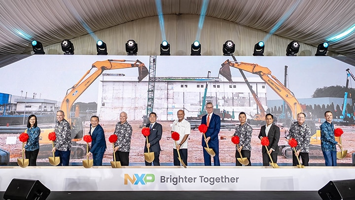
NXP Semiconductors has broken ground on an expansion of its assembly and test operation in Petaling Jaya, Malaysia, adding approximately 500,000 square feet of production space to its existing semiconductor manufacturing site. Production is expected to begin ramping in the first quarter of 2028, with total site output projected to more than double once the new factory is fully operational.
The project will take NXP’s Petaling Jaya production footprint to around 900,000 square feet. The operation supports assembly and electrical testing across the company’s semiconductor portfolio, covering the back-end manufacturing steps that turn processed die into packaged and qualified devices ready for customer supply chains.
NXP plans to equip the new factory with automated material handling systems and advanced quality-management technologies. Those systems are intended to improve movement between process stages, strengthen traceability and increase manufacturing efficiency as the site handles a larger volume and mix of products.
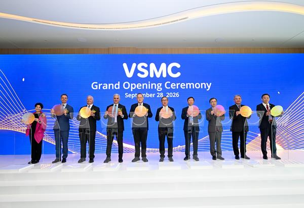
The expansion forms part of NXP’s hybrid manufacturing strategy, which combines internal production with foundry and manufacturing partnerships. Additional capacity in Malaysia is expected to support future output from the VSMC joint venture in Singapore and the ESMC joint venture in Dresden, Germany, linking back-end expansion directly with new front-end wafer capacity elsewhere in the network.
That connection is important because semiconductor capacity does not end at wafer fabrication. Finished wafers still need to be separated, packaged, inspected and electrically tested, and the available capacity at those stages determines how quickly additional wafer output can become qualified products. Packaging, thermal behaviour and test coverage are particularly important for automotive and industrial components, where operating conditions and long product lifecycles place heavier demands on qualification.
NXP serves automotive, industrial and IoT, mobile, and communications infrastructure markets. Devices used in those sectors often remain designed into equipment for years, making continuity of manufacturing and test capacity a practical part of component availability. A larger internal back-end footprint gives NXP another way to balance that requirement alongside external manufacturing partners.
Malaysia has formed part of NXP’s manufacturing base since 1972 and is already a major semiconductor assembly and test location. Expanding an established site allows the company to add capacity around an existing workforce, supplier ecosystem and manufacturing infrastructure rather than building the operation from scratch in a new region.
The Petaling Jaya project also broadens NXP’s geographic distribution. The company operates assembly and test capacity in Greater China and Thailand, while the Malaysian addition increases its ability to spread back-end production across several Asian locations. Its hybrid strategy combines that internal network with external manufacturing to avoid placing every stage of production within a single geography or supplier relationship.
Automation will influence how much effective capacity the new floor space produces. Material handling in assembly and test involves repeated movement between packaging, inspection and electrical-test equipment, and automated systems can reduce manual transfers while improving lot tracking and process consistency. Those gains become increasingly valuable as factories deal with high device volumes and a wide product mix.
The construction and installation programme still leaves a substantial period before additional output reaches customers. NXP expects the first production ramp during the opening quarter of 2028, after the building, equipment and manufacturing processes have been installed and qualified. At full operation, the company expects Petaling Jaya’s output to more than double, giving its growing wafer-manufacturing network substantially more internal capacity at the final stages of semiconductor production.