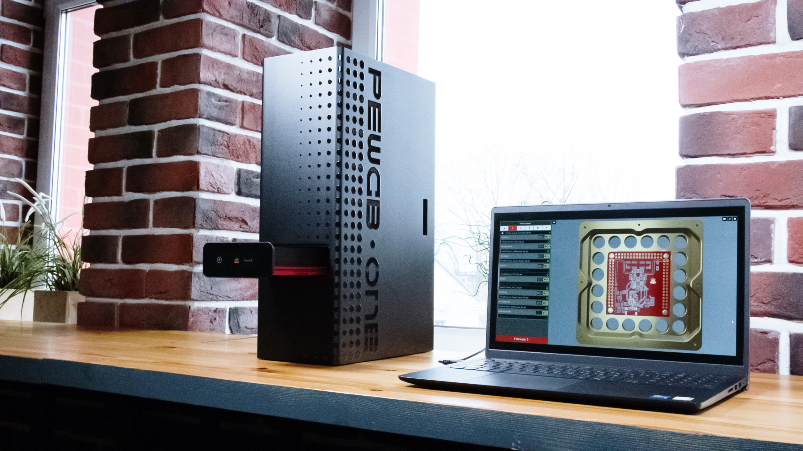
IN Brief:
- PewCB One uses a 20W, 1064nm pulsed laser with 35µm spot diameter and 30µm repeatability.
- Prepared double-sided ceramic blanks provide plated vias and through-holes without wet chemical processing or electroplating.
- The system specifies 0.1mm traces and spacing, supports 0201 components, and incorporates automatic stencil cutting and Class 1 laser containment.
PewCB has introduced a desktop printed-circuit-board prototyping system intended to shorten the interval between completing a PCB layout and testing assembled hardware. PewCB One combines laser ablation, prepared double-sided ceramic blanks, and automatic solder-paste stencil cutting, with the company specifying a design-to-test workflow of roughly 30 minutes for suitable boards.
The machine uses a 1064nm pulsed laser with 20W average optical power, a pulse duration of approximately 100ns, and a 35µm spot diameter. PewCB specifies 30µm positioning repeatability, 2µm resolution, and guaranteed minimum trace width and spacing of 0.1mm.
Those dimensions allow the system to accommodate relatively dense prototype layouts, including 0201 passive components and QFN packages with pitches of 0.5mm and below. PewCB also positions the process for compact digital and RF circuits, although the available board area and fixed via structure impose different layout constraints from conventional fabrication.
The blanks are fundamental to the process. Instead of starting with ordinary copper-clad laminate and creating every interlayer connection during fabrication, PewCB uses double-sided boards containing a predefined grid of metallised vias and rows of plated through-holes around the perimeter. Designers use templates within their EDA software and route signals towards the nearest available via when changing layers.
That arrangement removes drilling, electroplating, and wet chemical processing from the standard double-sided workflow. The blanks also arrive with solder mask already applied, allowing the laser to remove selected mask, copper, and substrate material to create the required pads and tracks.
The resulting layout freedom is not identical to a conventionally manufactured PCB. Via positions are largely dictated by the existing grid, although PewCB says an additional hole can be laser-drilled and fitted manually with a rivet where an interconnect is required outside the prepared pattern. For early circuit validation, that restriction trades some routing freedom for a much shorter fabrication process.
PewCB currently specifies blank dimensions from 23mm × 23mm to 84mm × 84mm. Supported materials include copper-clad alumina and zirconia ceramics rather than standard FR-4, giving the prototype a different mechanical and thermal structure from many production boards.
The ceramic substrate is useful during hot-plate or oven reflow because it distributes heat effectively, but the same property can make hand soldering more difficult. PewCB notes that alumina can draw heat away from larger pads rapidly enough to make a conventional soldering iron ineffective and recommends hot air, bottom-side preheating, or reflow for those assemblies. Zirconia blanks provide lower thermal conductivity where required.
Once the copper pattern has been fabricated, the same machine can cut the solder-paste stencil. The operator attaches a single-use tin stencil sheet directly to the PCB, returns the assembly to the tray, and the laser cuts apertures from the Gerber paste layer. Because the stencil remains attached to the board during cutting and paste application, no separate fiducial-alignment fixture is required.
Combining those processes addresses a significant part of the practical delay in rapid prototyping. Producing a bare board quickly has limited value if fine-pitch components then have to be hand soldered or an external stencil ordered separately. An aligned stencil allows paste deposition, component placement, and reflow to follow the board-fabrication step without another manufacturing lead time.
The process does introduce assembly considerations. Laser removal around tracks can leave the side edges of copper exposed where solder mask has also been removed, increasing the risk that excessive solder paste spreads beyond fine-pitch pads. PewCB recommends controlled paste deposition through its stencil system and allows additional UV-curable solder mask to be applied where necessary.
Automatic optical calibration is carried out before each run. PewCB uses a photodetector array to compensate for optical distortion and maintain beam position across the work area, a necessary control where tens of micrometres of positioning error can affect registration around compact pads and tracks.
The mechanical enclosure is designed around desktop rather than workshop use. PewCB One measures 155mm × 290mm × 464mm, weighs 11kg, and consumes up to 200W from a 110–230V AC supply. The laser is contained inside a fully enclosed metal chassis designed to comply with Class 1 laser safety requirements, with interlocks preventing operation unless the working chamber is closed.
Laser ablation also generates dust and fumes, so the machine incorporates G4 pre-filtration, an F7 fine filter, and activated carbon. Filter life is monitored by the software, while an internal camera allows the process to be observed without opening the enclosure.
The system is therefore aimed at a different part of the development cycle from a production PCB fabrication line. Its maximum board dimensions, predefined via grid, and ceramic substrate make it unsuitable as a direct substitute for unrestricted multilayer manufacturing, but those limitations matter less when the purpose is to validate an individual circuit before committing a complete design to an external board house.
Power converters, sensor interfaces, motor-control stages, adapter boards, measurement circuits, and other subsystems can be fabricated separately and tested before integration into a larger product. Several physical revisions can potentially be produced during the period normally occupied by fabrication and shipping of a single externally manufactured prototype.
PewCB currently lists the system at $5,000 under its Early Bird programme, including 20 starter blanks, with a 30% reservation deposit and an estimated delivery period of approximately 60 days. Shipping, import duties, and local taxes are additional.
The more consequential specification is the iteration time rather than the purchase price. PCB prototyping normally forces engineers to decide when a circuit is sufficiently mature to justify another fabrication cycle. A desktop process capable of producing 0.1mm features, plated interlayer connections, and an aligned assembly stencil changes that calculation by making another physical revision substantially quicker to obtain.