
IN Brief:
- Samsung will deploy customised Mistral AI models across semiconductor engineering and manufacturing operations.
- Initial applications include defect detection, equipment optimisation, shorter development cycles, and yield stabilisation.
- The on-premises architecture keeps sensitive semiconductor process and operational data within Samsung infrastructure.
Samsung Electronics has entered a strategic partnership with Mistral AI to deploy on-premises artificial intelligence across semiconductor engineering and manufacturing, with customised models intended to operate inside Samsung infrastructure rather than moving sensitive process data into external cloud services.
The agreement includes Mistral’s flagship Mistral Large model and covers AI systems tailored to semiconductor workloads. Samsung has also led Mistral AI’s Series D funding round and taken a strategic equity stake, tying the engineering collaboration to a broader commercial relationship.
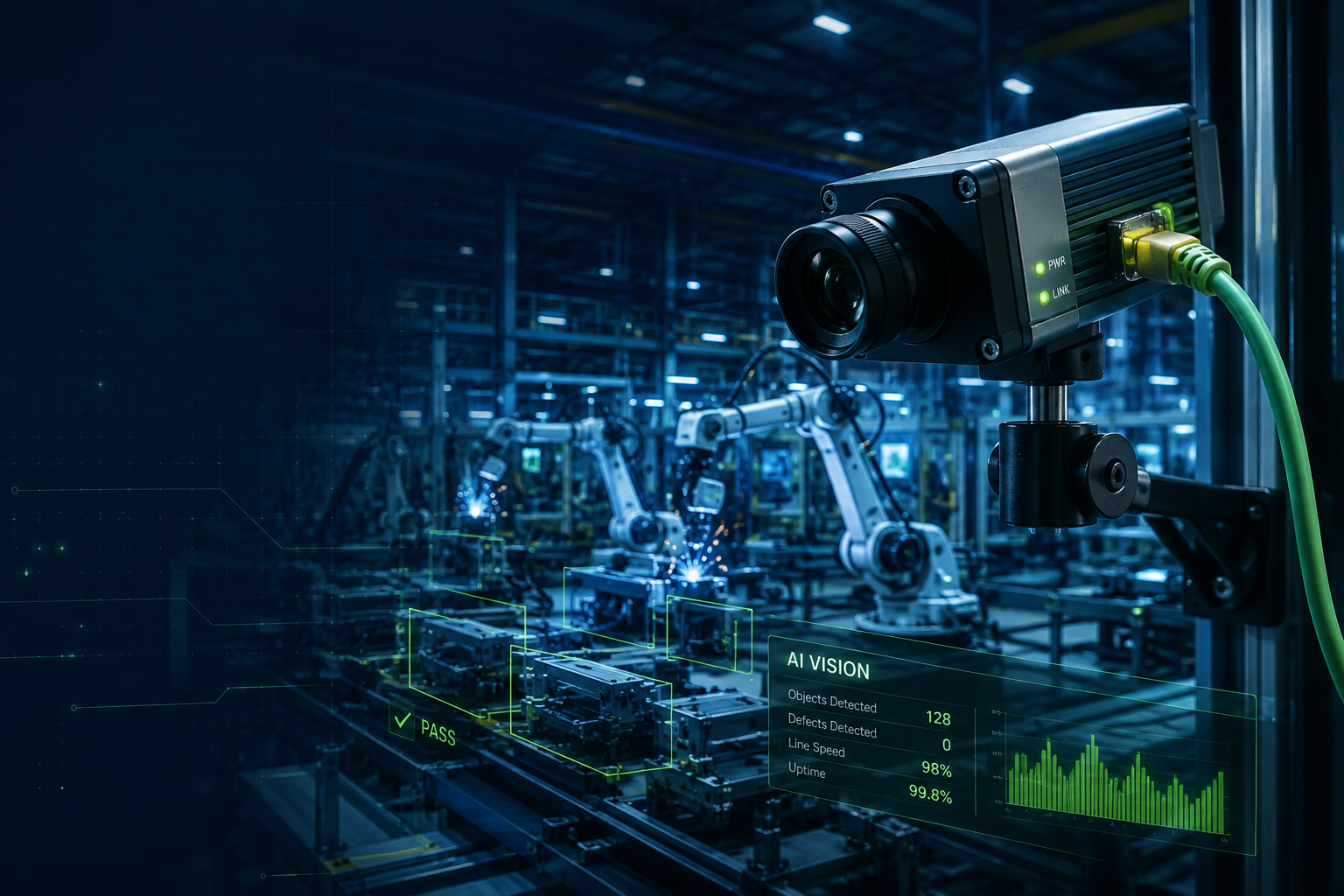
Samsung has identified defect detection and equipment optimisation among the initial manufacturing applications, alongside shorter development cycles, improved manufacturing precision, and more stable yields. Modern fabs generate extensive inspection, metrology, tool-state, maintenance, and process data, making the quality of the links between those datasets and engineering decisions as important as the AI model itself.
Young Hyun Jun, Vice Chairman and CEO of Samsung Electronics’ Device Solutions division, said: “Increasing complexities involved in AI chip design and manufacturing requires continuous innovation in semiconductor technologies.” The Device Solutions division encompasses Samsung’s memory, foundry, and system semiconductor operations, placing the work directly inside its chip-design and manufacturing organisation.
An on-premises architecture also addresses the sensitivity of semiconductor manufacturing data. Process recipes, design information, equipment behaviour, yield data, and failure signatures can contain substantial intellectual property, while some operational datasets are unsuitable for processing outside tightly controlled infrastructure. Local deployment gives Samsung greater control over data retention, system access, and integration with existing fab systems.
The project arrives as manufacturing complexity is increasing elsewhere in Samsung’s roadmap. The company is targeting High-NA EUV for DRAM high-volume manufacturing by 2028 and is participating in development of a larger 12-inch photomask platform, as detailed in Samsung’s High-NA manufacturing programme. Higher-resolution lithography brings its own requirements around masks, metrology, process control, overlay, and yield management.
Semiconductor plants already depend heavily on statistical process control, equipment monitoring, machine vision, and advanced process-control systems. The new AI layer is more likely to complement those established tools than replace deterministic control systems, particularly where engineers need to interrogate complex datasets, retrieve technical knowledge, identify recurring signatures, or accelerate fault diagnosis.
That distinction will be important once the models reach production environments. Generative and analytical AI can make large engineering datasets easier to navigate, but fab decisions still depend on traceable measurements, controlled processes, and repeatable results. Samsung has not said that Mistral models will directly control manufacturing equipment, nor has it disclosed the compute architecture supporting individual deployments.
Mistral’s role also reflects growing demand for AI models that can operate within controlled enterprise infrastructure. Semiconductor manufacturing is a demanding test case because data security has to coexist with high availability, long equipment lifecycles, and engineering systems that cannot tolerate casual changes to production behaviour.
The companies have not disclosed deployment scale, individual fab locations, or quantified performance targets. Results in defect analysis, equipment availability, engineering cycle time, and yield will provide the more useful measure of whether the partnership adds value beyond the additional software layer.
