
IN Brief:
- CEA-Leti, Spintec, and C2N researchers combined HfO₂ ReRAM with stochastic magnetic tunnel junctions.
- The shared read voltage controls both memristive coupling and magnetic-device stochasticity to provide intrinsic annealing.
- The prototype solved 24-vertex MAX-CUT and 10-vertex graph-colouring benchmarks, while larger parallel systems remain future work.
CEA-Leti, Spintec, and C2N/Université Paris-Saclay researchers have demonstrated a hybrid nanoelectronic Ising machine combining hafnium-oxide resistive memory with stochastic magnetic tunnel junctions. The architecture uses the physical behaviour of both device types to store problem couplings, generate probabilistic spin states, and control annealing during combinatorial optimisation.
CEA-Leti issued its current research communication on 8 September 2026. The underlying peer-reviewed paper, Intrinsic annealing in a hybrid memristor-magnetic tunnel junction Ising machine, was published in Nature Communications on 16 April 2026, so the September announcement concerns the demonstrated architecture rather than the first publication of the research.
An Ising machine maps an optimisation problem onto interacting binary variables and searches for a low-energy configuration representing a useful solution. Electronic implementations are intended to reduce some of the instruction and data-movement overhead involved when the same search behaviour is simulated conventionally in software.
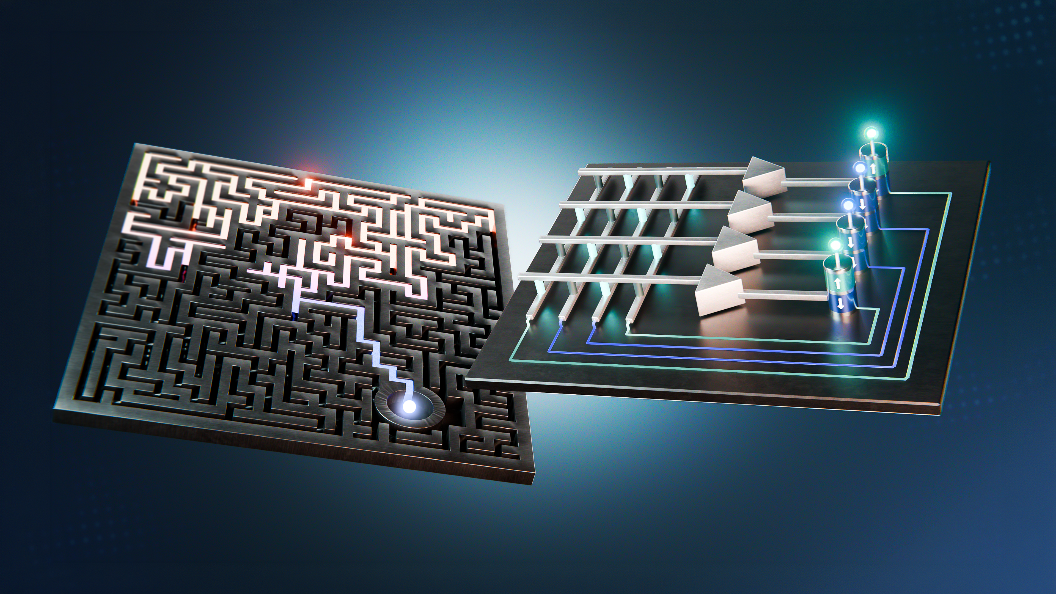
The French team’s hardware divides the calculation between two nanotechnologies. A hafnium-oxide ReRAM crossbar stores multilevel coupling values describing how the variables interact, while stochastic magnetic tunnel junctions act as thermally fluctuating binary spins.
The unusual part of the design is the way those devices are electrically linked. The same read voltage used to interrogate the memristor crossbar also influences the stochastic switching behaviour of the SMTJs. At lower read voltage, the magnetic devices fluctuate more readily; increasing the voltage makes their state increasingly deterministic.
That behaviour gives the machine an intrinsic annealing mechanism. Optimisation searches typically benefit from greater stochasticity early in the process because it allows the system to escape local minima, followed by progressively lower randomness as it converges on a stable solution. The hybrid architecture adjusts that balance with the common read voltage rather than requiring a separate digital control operation for every update.
The prototype was tested on a 24-vertex weighted MAX-CUT problem and a 10-vertex, three-colour graph-colouring problem. The researchers report that it consistently reached the global optimum in both cases, with measurements performed at room temperature and without an external magnetic field.
The demonstrations are still small compared with industrial optimisation workloads. The full annealing experiments also used a computer-mediated feedback configuration, with the memristor array evaluated before a controller calculated and applied the corresponding voltage to the SMTJ. The paper separately demonstrates direct analogue coupling between the array and magnetic device, but the benchmark machine is not yet a fully integrated parallel accelerator.
That distinction limits claims about system-level speed and energy efficiency. The research establishes that the two device types can operate together and that their interaction provides a useful annealing mechanism; it does not yet provide a large-scale benchmark showing an energy or time-to-solution advantage over conventional processors or competing optimisation accelerators.
The integration route is nevertheless relevant to scaling. Both the memristor array and SMTJs are fabricated above CMOS circuitry in back-end-of-line structures, although they currently reside on separate dies. That opens a possible route towards vertical integration in which memory, probabilistic devices, and control electronics are placed closer together.
Shorter interconnects and parallel operation could reduce the conversion and data-movement overhead that remains in the experimental system. The research team identifies closer control-electronics integration, larger problem sizes, genuine parallel updates, and direct benchmarking against conventional computing as priorities for the next phase.
The target applications extend beyond one computing market because combinatorial optimisation appears in logistics routing, power-grid management, industrial scheduling, chip design, and computing-resource allocation. Those applications will require problem sizes far beyond the present demonstrations, making device variability, interconnect scaling, error behaviour, and parallel update architecture as important as the individual switching speed of the nanodevices.
The current result establishes a working connection between dense resistive-memory couplings and thermally driven magnetic variables, with a shared electrical parameter controlling the search temperature. The next measure of the architecture will be whether that device-level elegance survives larger arrays and removes enough external control overhead to produce a measurable system advantage.
