IN Brief:
- Soitec is negotiating multi-year capacity agreements with more than ten photonics-SOI customers.
- Contracts use fixed pricing and staged deposits tied to committed wafer volumes, alongside customer inventory reporting.
- Existing French and Singapore facilities are expected to cover near-term growth before any requirement for a new fabrication plant.
Soitec is moving its silicon-photonics customers onto multi-year capacity agreements with fixed pricing and financial deposits as demand for optical interconnect hardware accelerates around AI data-centre infrastructure.
The French engineered-substrate manufacturer is negotiating agreements with more than ten photonics customers. Around 80% of those capacity reservations are expected to be signed within one or two weeks, with the balance following within roughly a month, according to chief executive Laurent Rémont.
The contracts are designed to turn customer forecasts into firmer production commitments. Buyers place deposits against agreed wafer volumes, with the money returned when those volumes are taken. Customers that fall short lose the relevant deposit, while demand above the contracted quantity triggers a new pricing discussion.
Soitec is also requiring customers to provide inventory information, giving the substrate manufacturer greater visibility of actual consumption rather than relying only on orders placed further up the supply chain. That becomes particularly important when shortages encourage customers to reserve more capacity than they genuinely expect to use.
The shift reflects a substantial change in the company’s photonics business. Soitec previously indicated that revenue from photonics-SOI substrates would more than double during its current financial year from a level slightly above $100 million. Rémont now regards revenue above $200 million as a floor rather than an upper-end scenario.
Silicon photonics is becoming increasingly important in AI systems because moving data between processors, accelerators, switches, memory, and neighbouring racks is consuming a larger share of the available system power budget. High-speed copper links become progressively harder to extend as signalling rates rise, increasing the attraction of optical connections where bandwidth, reach, and energy per bit become more restrictive.
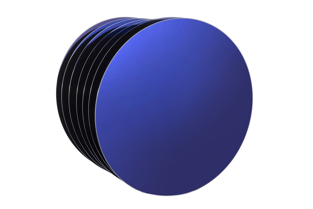
Soitec’s photonics-SOI material provides the starting substrate for many of those optical integrated circuits. The structure combines a controlled single-crystal silicon device layer with a buried oxide layer and silicon handle wafer, giving photonic designers a platform for fabricating waveguides, modulators, coupling structures, photodetector integration, and associated optical circuitry.
The quality of that starting material has direct consequences for the finished optical device. Thickness control and surface roughness influence waveguide behaviour and optical loss, while wafer flatness, defect density, and mechanical stability affect semiconductor processing, packaging, and fibre attachment later in manufacture.
That makes additional substrate capacity more complicated than simply increasing square metres of cleanroom space. New production equipment has to deliver material that remains sufficiently close to previously qualified wafers for customers to use without introducing unacceptable process variation or forcing lengthy requalification programmes.
Soitec has an unusually strong position in this part of the supply chain. UBS estimates that the company accounts for around 95% of the market for substrates underpinning silicon-photonics devices, leaving customers particularly exposed to its available capacity as optical networking volumes rise.
The company is attempting to meet that demand without immediately committing to another fabrication plant. Rémont does not expect a completely new fab to be required before around 2029, with Soitec instead using capacity already available across its manufacturing network.
Two expansion routes are already under way. The company can shift production between businesses that share underutilised manufacturing infrastructure, while additional tools can be installed in cleanroom space that is already built. Soitec expects those measures to cover demand during the current year and the following one.
Some of that flexibility comes from French cleanroom capacity originally developed for silicon-carbide production. Reusing existing infrastructure shortens the route to additional wafer output because buildings, utilities, contamination controls, and supporting services are already in place, although production equipment still has to be installed, commissioned, and qualified for photonics-SOI.
The geographical manufacturing base has also widened. Photonics-SOI had been produced only in France until earlier this year, but Soitec has since qualified customers for output from its Pasir Ris operation in Singapore. The site already supports several SOI technologies and provides another route for increasing 300mm substrate production.
A further Singapore expansion remains available if demand continues to strengthen. Soitec has an existing but unequipped building that could be fitted out rather than constructing another fab from the ground up. A decision on whether to equip that building is expected within the next six to 12 months.
Those options give Soitec more flexibility than a conventional greenfield expansion, but they do not eliminate the manufacturing challenge. Photonics customers need consistent device-layer thickness, surface condition, defect performance, and wafer geometry regardless of which Soitec line produces the substrate.
Capacity agreements therefore serve two purposes. They give Soitec evidence that customers genuinely require the additional output before equipment spending is committed, while fixed prices and deposits reduce the commercial risk of reserving cleanroom and tool capacity for forecasts that may later disappear.
The arrangement also places more responsibility on customers to forecast accurately. AI infrastructure demand is rising quickly, but optical architectures are evolving just as rapidly between pluggable transceivers, near-packaged optics, and co-packaged systems. A supplier reserving wafers several years ahead has to balance genuine growth against the risk of customers protecting themselves with overlapping orders.
Soitec’s inventory-reporting requirement is aimed directly at that behaviour. Better visibility of customers’ stock levels should allow the company to distinguish between wafers moving into production and material accumulating as precautionary inventory, an important difference when deciding whether another cleanroom or fabrication building is actually required.
For now, the company is relying on existing French and Singapore infrastructure rather than another greenfield fab. The harder test will arrive as contracted demand converts into real wafer starts: maintaining substrate quality and customer qualification while photonics-SOI revenue moves beyond $200 million and optical interconnects become a materially larger part of AI hardware production.