
IN Brief:
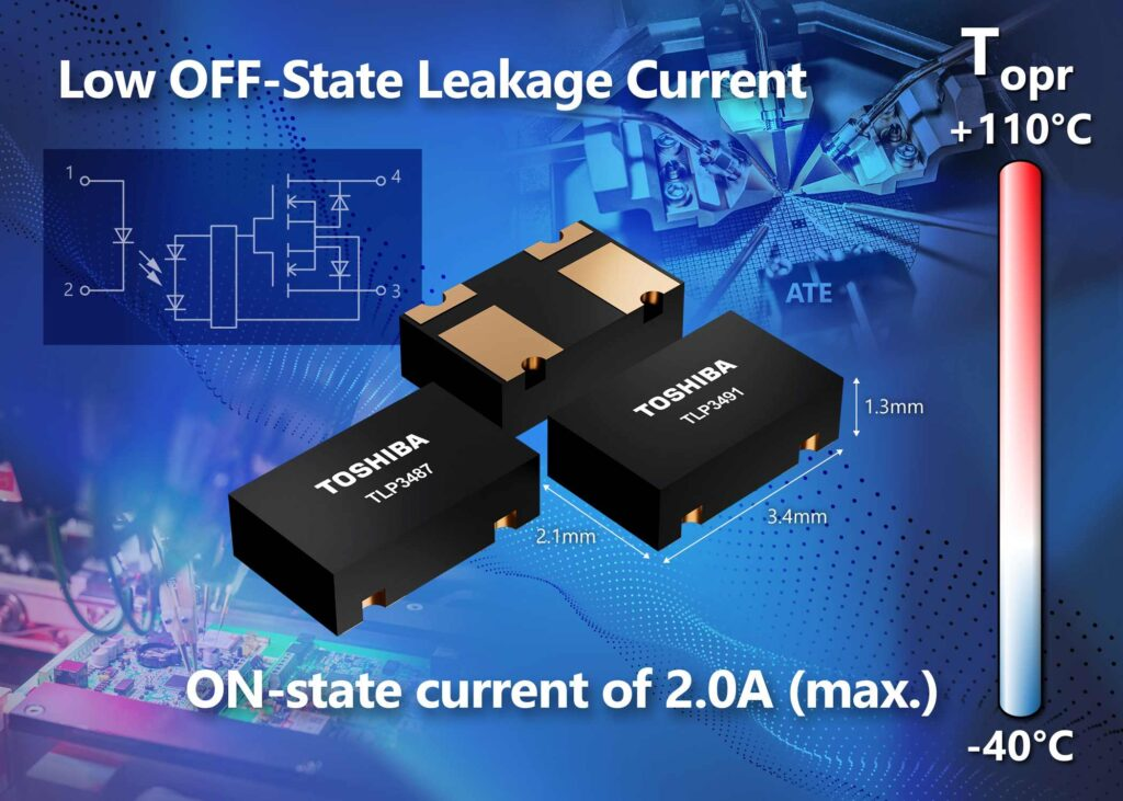
- The TLP3487 and TLP3491 photorelays provide a maximum on state current of 2A.
- Off state leakage is specified at 10nA or 1nA, depending on the device.
- Compact P-SON4 packaging supports denser switching matrices in automated semiconductor test equipment.
Toshiba Electronic Devices & Storage has introduced two compact photorelays for signal and power path switching in semiconductor automatic test equipment and precision measurement systems. The TLP3487 and TLP3491 occupy a P-SON4 package measuring 3.4mm × 2.1mm × 1.3mm, while both support a maximum on state current of 2A.
Different voltage and leakage characteristics allow the devices to address separate measurement requirements. The TLP3487 supports an off state output terminal voltage of 60V with maximum leakage of 10nA, whereas the TLP3491 is rated at 40V and reduces maximum leakage to 1nA.
Such leakage becomes significant when a switching matrix sits between precision instrumentation and a device under test. Current passing through a nominally open path can distort a measurement, disturb a high impedance node, or make it difficult to separate device behaviour from errors introduced by the test interface.
Optical isolation separates the input and output stages, removing the mechanical contacts used in conventional relays. Contact bounce and mechanical wear are consequently eliminated, while the components can be assembled using standard semiconductor mounting processes within densely populated test boards.
Compared with a 2.54SOP4 package, the P-SON4 format reduces mounting area by about 74%; against a 2.54SOP6 package, the reduction reaches roughly 84%. Operation is specified from -40°C to 110°C, accommodating the local heating and enclosure temperatures found in heavily populated automated test systems.
The relays are intended for memory, system on chip, and mixed signal test equipment, where large switching matrices route precision supplies, digital signals, analogue measurements, and parametric tests between instruments and several devices under test. Their compact dimensions also suit laboratory instruments that need more channels within a fixed enclosure.
Channel density raises the value of every millimetre
Semiconductor complexity is increasing the number of pins, voltage domains, interfaces, and test conditions handled by each platform. When hundreds or thousands of relay channels are used, a small reduction in component footprint can release meaningful board area for shorter signal paths, additional sites, monitoring circuitry, or improved separation between sensitive analogue and noisy digital sections.
Parallel test adds further pressure because each extra site multiplies the required switching and instrumentation. Higher site counts improve equipment utilisation and reduce test cost per device, yet they also increase routing congestion, power dissipation, calibration work, and the opportunity for channels to interact.
Although package size is important, it cannot determine the suitability of a photorelay on its own. On resistance affects voltage drop and dissipation under load, while output capacitance influences high frequency isolation and settling behaviour; switching time, thermal drift, parasitic coupling, and lifetime stability must all fit within the measurement uncertainty and throughput required by the application.
A Yokogawa analyser developed for direct measurement at 2,000V DC demonstrates how test instruments are expanding to handle higher voltage and more complex power conversion. Preserving that capability requires a switching network whose leakage, resistance, and capacitance remain below the measurement error budget.
As chiplets and heterogeneous packages broaden the problem, the switching architecture must accommodate a wider range of electrical behaviour. Logic, memory, analogue, RF, and power management functions can coexist within one assembly, forcing the test system to manage very different stimulus levels, bandwidths, isolation requirements, and measurement techniques through a common interface.
Dense solid state switching can help, although careful load board design remains indispensable. Guarding, grounding, thermal control, calibration, signal integrity, and the physical arrangement of return paths still decide whether the full instrument accuracy reaches the device pins.
Toshiba’s two relays provide a smaller switching element with characteristics tailored to precision test, allowing developers to trade voltage rating against leakage while retaining the same package and current capability. Their contribution will be measured across the complete matrix, where thousands of modest savings in space and error can produce a materially denser and more accurate test system.

